FABLESS:
The Transformation of The
Semiconductor Industry
DANIEL NENNI
PAUL MCLELLAN
WITH FOREWORD BY CLIFF HOU
VP OF R&D, TSMC
A SEMIWIKI.COM PROJECT
Fabless: The Transformation of the Semiconductor Industry
Copyright 2019 by SemiWiki.com LLC. All rights reserved. Printed in the United
States of America. Except as permitted under the United States Copyright Act of 1976,
no part of this publication may be reproduced or distributed in any form or by any
means or stored in a database or retrieval system without the prior written consent of
the publisher.
Authors: Daniel Nenni and Paul McLellan
Editors: Beth Martin and Amanda Ketchum
ISBN-13: 978-1497525047
ISBN-10: 1497525047
BISAC: Business & Economics / General
3
4
Table of Contents
Introduction ...................................................................................................................... 7
Foreword............................................................................................................................ 9
Preface .............................................................................................................................. 11
Chapter 1: The Semiconductor Century ..................................................................... 15
Chapter 2: The ASIC Business ..................................................................................... 27
In Their Own Words: VLSI Technology ............................................................................ 35
In Their Own Words: eSilicon Corporation ....................................................................... 43
2019 Update: eSilicon Corporation ...................................................................................... 51
Chapter 3: The FPGA .................................................................................................... 57
Update 2019: FPGA Landscape ........................................................................................... 65
In Their Own Words: Xilinx ................................................................................................. 69
In Their Own Words: Achronix ........................................................................................... 83
Chapter 4: Moving to the Fabless Model .................................................................... 95
In Their Own Words: Chips and Technologies ............................................................... 101
Chapter 5: The Rise of the Foundry .......................................................................... 105
2019 Update: Foundries ....................................................................................................... 113
In Their Own Words: TSMC and Open Innovation Platform ..................................... 121
2019 Update: TSMC ............................................................................................................. 133
2019 Update: Dr. Morris Chang ......................................................................................... 147
In Their Own Words: GLOBALFOUNDRIES ..................................................... 149
2019 Update: GLOBALFOUNDRIES ............................................................................. 159
Chapter 6: Electronic Design Automation ............................................................... 169
2019 Update: EDA ............................................................................................................... 181
In Their Own Words: Mentor Graphics ........................................................................... 185
2019 Update: Mentor Graphics .......................................................................................... 201
In Their Own Words: Cadence Design Systems .............................................................. 205
2019 Update: Cadence .......................................................................................................... 221
5
In Their Own Words: Synopsys ......................................................................................... 227
2019 Update: Synopsys ......................................................................................................... 243
Chapter 7: Intellectual Property ................................................................................. 249
2019 Update: Semiconductor IP ......................................................................................... 257
2019 Update: In Their Own Words: ARM ....................................................................... 261
In Their Own Words: Imagination Technologies............................................................ 271
2019 Update: Wave Computing and MIPS Technologies .............................................. 285
2019 Update: IP Management ............................................................................................. 291
In Their Own Words: Methodics ....................................................................................... 295
Chapter 8: What’s Next for the Semiconductor Industry? ..................................... 299
6
7
Introduction
Paul McLellan, Daniel Payne, and I have more than 100 years of
combined experience in the semiconductor industry. We started sharing
our observations, opinions, and experiences when semiconductor blogging
was just getting started. Many semiconductor bloggers followed, peaking at
more than 200 in 2010. We literally brought blogging to the semiconductor
industry, which was very disruptive at the time. Blogging is hard work and
only the company (employee) bloggers would survive without independent
blogger compensation. In 2011 Paul, Daniel, and I joined our blogs
together to create a crowdsourcing platform (SemiWiki.com) to not only
appeal to a wider audience, but to also get compensated for our efforts.
At first we were chastised for pretending to be journalists, in fact we were
not allowed press passes or access to press rooms at conferences. The tide
turned, of course, and now blogging is the media mainstay for all industries
including semiconductors. Don’t be fooled by fancy executive editor titles,
the majority of the news today is written by people like us who share
observations, experience, and opinions. The difference of course is that
most mainstream semiconductor bloggers do not have deep semiconductor
experience like the SemiWiki contributors.
Dozens of people have blogged on SemiWiki and more than three
million people have visited. SemiWiki has published more than five
thousand blogs since 2011 garnering more than thirty-three million views.
The result is a trove of content and analytics of who reads what, when,
where, how, and why. Several of the regular SemiWiki bloggers have
8
launched off into bigger and better things but most are still here to stay
active in the industry that we all love.
On June 1
st
, 2019 we launched SemiWiki 2.0 which includes an IP
Enablement Portal. We will talk about this more in the Semiconductor IP
Chapter update so keep reading. It will be another SemiWiki disruption and
we hope you will be part of it, absolutely.
SemiWiki has also published seven books, with more planned. This
particular book started it all when Paul McLellan, Beth Martin, and I
decided to document the history of the fabless semiconductor industry as
published on SemiWiki.com. It was a labor of love since we posted a free
PDF version and have given away thousands of print copies over the last
six years.
A lot has happened in the semiconductor ecosystem since we first
published in 2013 so we decided to do a revised edition. It has grown more
than 50 pages and includes updates from eSilicon, Synopsys, Mentor
Siemens, Cadence, ARM, and new "In Their Own Words" entries from
Achronix, Methodics, and Wave/MIPS. Also included are industry updates
on: FPGA, Foundry, EDA, IP, TSMC, GLOBALFOUNDRIES,
and a new subchapter on IP Management. Most importantly there is a
NEW chapter 8: “What’s Next for the Semiconductor Industry” written by
EDA icon Dr. Walden Rhines. Thank you again for reading and I hope to
see you on www.SemiWiki.com.
Daniel Nenni
CEO, Founder, SemiWiki.com LLC June 2019
9
Foreword
Dr. Cliff Hou, Vice President, Research and Development, TSMC
Semiconductor innovation has the power to change the world. Although,
well over half a century ago, when semiconductors first came into being,
few people really saw that promise. That power of semiconductors to
innovate has stretched beyond its original applications. It also has changed
how semiconductors are manufactured.
Over the first 30 years of its existence, the semiconductor industry
followed the proven integrated manufacturing model of the time. Those
companies who owned the manufacturing assets made, marketed,
researched and developed their own products. But then, the dynamics of
innovation mingled with laws of supply and demand and a new concept—
outsourcing—emerged and gave birth to what is known today as the
dedicated foundry model, and the world has never been the same.
Dr. Morris Chang is credited with identifying the innovation need and
providing the resources to meet it. The need was making available
manufacturing resources that are 100 percent dedicated to those emerging
semiconductor companies that lacked the financial wherewithal to own
their own expensive equipment. Like all great ideas, the premise was simple.
What no one foresaw is that it would give rise to two, if not three, new
industry segments, all of which contribute greatly to the innovative spirit
of the industry today.
10
When Dr. Chang established the Taiwan Semiconductor Manufacturing
Company (TSMC) in 1987, the foundry segment and the fabless
semiconductor model were born. Today, fabless semiconductor
companies—those companies who do not own manufacturing
resources—are the fountainhead of innovation that is the foundation for
our electronic world. The foundry segment has allowed these companies to
invest in design and innovation rather than in manufacturing. As a result,
innovation and the world economy have raced forward at an
unprecedented pace. This has given nearly every semiconductor company
the flexibility to innovate widely and creatively, constantly expanding the
universe of products we rely upon today.
Equally remarkable has been the rise of a powerful design ecosystem to
complement the fabless industry. The ecosystem works in unison with
designers and foundries to ensure that the IP, design tools, and services
needed to get next-generation designs taped-out and in production are
proven and ready to help customers meet their time-to-market goals.
Today, the emergence of the fabless model, the dedicated foundry industry
segment and an independent design ecosystem are driving the mobile
revolution and will be the foundation of the internet-of-things.
Even as this book was being written, the semiconductor industry
continued to evolve. The drive to integrate the design and manufacturing
links in the semiconductor value chain is now being extended downstream (to
manufacturing equipment and materials suppliers) and upstream to major
product companies. This is taking on the power of integration— virtual
integration. Virtual integration is, by definition, the power of collaboration
that blazes the direction and vision for the next generation of innovation.
Innovation will always be the hallmark of the semiconductor industry
and it is the theme that runs through this book. I’m honored and humbled
to be part of this exciting industry and equally honored and humbled to
offer my comments as the introduction to this book.
Dr. Cliff Hou, January 2014
11
Preface
The purpose of this book is to illustrate the magnificence of the fabless
semiconductor ecosystem, and to give credit where credit is due.
We trace the history of the semiconductor industry from both a technical
and business perspective. We argue that the development of the fabless
business model was a key enabler of the growth in semiconductors since the
mid-1980s. Because business models, as much as the technology, are what
keep us thrilled with new gadgets year after year, we focus on the evolution
of the electronics business.
We also invited key players in the industry to contribute chapters. These
“In Their Own Words” chapters allow the heavyweights of the industry to
tell their corporate history for themselves, focusing on the industry
developments (both in technology and business models) that made them
successful, and how they in turn drive the further evolution of the
semiconductor industry.
Before we dive in, let’s define some terms. Rather than electronics, which
refers to whole devices like your cell phone or TV, we’ll be using the terms
chip, IC, ASIC, SoC, and FPGA throughout the book as we focus on the
components that go into the devices. Chip or IC can refer more broadly to
the two main types of semiconductor devices we cover: ASICs and SoCs
(systems-on-chip), and FPGAs (field-programmable gate arrays). We have
chosen not to cover many other electronic components including memory,
flash, mixed-signal technology, and micro-electro-mechanical systems
(MEMS).
12
We also talk about several phases of development in the semiconductor
industry, and use the following terms to describe the companies and
technologies that define a particular business model.
IC: An integrated circuit, also called a chip, is a set of electronic circuits,
including transistors and other components, on a silicon substrate.
Systems company: A systems company makes a consumer product
from chips that other companies have designed. Examples include Cisco
and Apple.
Semiconductor company: Also called integrated device manufacturer
(IDM), these companies, like Intel and Samsung, design and manufacture
standard ICs that systems companies use in their products. Until the mid-
1980s, all semiconductor companies were IDMs, that is, they controlled
both the design and manufacture of their chips. This changed gradually,
and now there are only a few (Intel and Samsung notably). All other chip
makers outsource the manufacturing of their designs to a foundry.
ASIC: Application specific integrated circuit refers to two things: a chip
that is custom designed for a specific application, rather than for a general-
purpose application, and to the type of company that developed in the
1980s that performed the physical design and manufacturing of these
application-specific ICs for other semiconductor or systems companies.
“ASIC” is now commonly used interchangeably with “IC.”
SoC: A system-on-chip is an IC that integrates all components of a
computer or other electronic system into a single chip. It may contain
digital, analog, mixed-signal, and often radio-frequency functions—all on a
single chip substrate.
Fabless company: A company that designs their own chip but
outsources the manufacturing to a third-party, either a pure-play foundry
or an IDM that sells excess fab capacity. This is the prevailing business
model today.
EDA: Electronic design automation companies make the software that
is used to design all modern semiconductor devices. The three dominant
13
EDA companies today are Synopsys, Cadence Design Systems, and Mentor
Graphics.
IP: Semiconductor intellectual property companies sell chip designs that
are implemented in their customer’s ASICs, SoCs, or other semiconductor
devices. A useful metaphor is that rather than selling a complete house, IP
companies sell you the blueprint. The best-known IP company is ARM.
Foundry: A business that is a dedicated semiconductor fabrication
facility that does not design its own ICs. The term “fab” refers to any
semiconductor fabrication plant, whether run as part of an IDM (like Intel)
or as a foundry (like TSMC).
The economics of designing a chip and getting it manufactured is similar
to how the pharmaceutical industry gets a new drug to market. Getting to
the stage that a drug can be shipped to your local pharmacy is enormously
expensive. But once it’s done, you have something that can be
manufactured for a few cents and sold for, perhaps, ten dollars. ICs are like
that, although for different reasons. Getting an IC designed and
manufactured is incredibly expensive, but then you have something that
can be manufactured for a few dollars, and put into products that can be
sold for hundreds of dollars. One way to look at it is that the first IC costs
many millions of dollars—you only make a lot of money if you sell a lot of
them.
What we hope you learn from this book is that even though IC-based
electronics are cheap and pervasive, they are not cheap or easy to make. It
takes teams of hundreds of design engineers to design an IC, and a complex
ecosystem of software, components, and services to make it happen. The
fabs that physically manufacture the ICs cost more to build than a nuclear
power plant. Yet year after year, for 40 years, the cost per transistor has
decreased in a steady and predictable curve. There are many reasons for
this cost reduction, and we argue that the fabless semiconductor business
model is among the most important of those reasons over the past three
decades.
14
The next chapter is an introduction to the history of the semiconductor
industry, including the invention of the basic building block of all modern
digital devices, the transistor, the invention of the integrated circuit, and the
businesses that developed around them.
15
Chapter 1: The Semiconductor
Century
Although the technology behind our electronic devices is largely hidden
from sight, its influence on our daily lives, our health, our economy, and our
entertainment is undeniable. Today, digital electronics are ubiquitous and
indispensable to the daily life of modern people. But it wasn’t always so.
Two big things happened to bring consumer electronics into every
household: the invention of the transistor in 1947, and the invention of the
integrated circuit (IC) in 1959. Then, lots of little things happened to make
ICs small and cheap enough to occupy nearly every aspect of our lives.
For the average western child in the 1950s and 1960s, the only electronics
in the household were the radio and the television, both of which contained
tubes (valves in some countries) not digital semiconductor technology. The
only widespread electronic product was the transistor radio, which you
could buy for roughly $20 ($150 in 2013 dollars).
In the 1970s, kids still watched analog TVs, but all radios were transistor
based and you could buy a pocket calculator (for about $160 in 2013
dollars), an early PC, digital watches, and an Atari game console. A kid in
the 1980s would also have a Walkman, a CD player, a VCR, video camera,
boom box, an electric typewriter, and maybe an actual IBM PC. Anyone
born after 1990 will probably not remember a time without cell phones,
flat panel TVs, GameBoys, laptops, and tablets. Electronics are now
16
incorporated into nearly everything from home thermostats and
toothbrushes, to cars and medical devices.
Today, an iPad has more processing power than a Cray supercomputer in
1990, which was the size of a refrigerator. Our cars contain dozens of
microprocessors. We shop online. We read books on tablets. We play video
games on consoles that are more powerful than the flight simulators of
twenty years ago. We’ll let futurists predict what electronics a child born in
2013 might never live without. It’s been a steep curve up and to the right
for the number and types of electronic devices we encounter daily.
The Invention of the Transistor and the Integrated Circuit
The transistor, which is just a switch that controls the flow of electrical
current in a computer chip, is at the heart of almost all electronics. This
makes it among the most important inventions of the 20th century. It was
invented at Bell Labs in New Jersey in 1947 by John Bardeen, Walter
Brattain, and William Shockley. Shockley then left Bell Labs and returned
to Palo Alto, CA, where he had been brought up. He opened Shockley
Semiconductor Laboratory as a division of Beckman Instruments, and tried
to lure ex-colleagues from Bell Labs to join him. When he was unsuccessful,
he searched universities for the brightest young graduates to build the new
company. This was truly the genesis of Silicon Valley and some of its culture
that still exists today. Shockley is credited with bringing the silicon to Silicon
Valley.
“What we didn’t realize then was that the
integrated circuit would reduce the cost of electronic
functions by a factor of a million to one, nothing
had ever done that for anything before” -Jack Kilby
Shockley’s management style was abrasive, and he alienated many who
worked for him. The final straw came when Shockley decided to
discontinue research into silicon-based transistors. Eight people, known as
the “traitorous eight,” resigned and with seed money from Fairchild
17
Camera and Instrument they created Fairchild Semiconductor Company.
Almost all semiconductor companies, notably Intel, AMD, and National
Semiconductor (now part of Texas Instruments) have their roots in
Fairchild in one way or another. For this reason, they were referred to as
“Fairchildren.” These companies drove the development of silicon-based
integrated circuits. Silicon wasn’t the only material in play for making
transistors, but it turned out to be the winning technology.
The next key invention came in 1959 from Jean Hoerni at Fairchild when
he created the “planar” manufacturing process, which flattened the
transistor and allowed it to be mass-produced. The same year, Jack Kilby
at Texas Instruments and Robert Noyce at Fairchild developed the
integrated circuit. The IC connected diodes, transistors, resistors, and
capacitors on a single silicon chip. Kilby and Noyce both received the
National Medal of Science, and Kilby received the Nobel Prize for the work
in 2000 (Noyce died in 1990).
The integrated circuit turned out to be the big breakthrough. Until that
point, transistors were built one at a time and wired together manually
using “flying-wire” connections. The planar manufacturing process allowed
multiple transistors to be created simultaneously and connected together
simultaneously. By 1962, Fairchild was producing integrated circuits with
about a dozen transistors. Much has changed in the intervening years, but
we use the same basic principle to build modern billion-transistor chips.
Those two inventions, the transistor and then the integrated circuit, are the
key to electronics today and all the ways in which electronics affects our
lives.
Moore’s Law
“The whole point of integrated circuits is to absorb the functions of
what previously were discrete electronic components, to incorporate
them in a single new chip, and then to give them back for free, or at
least for a lot less money than what they cost as individual parts.
18
Thus, semiconductor technology eats everything, and people who
oppose it get trampled.” -Gordon Moore
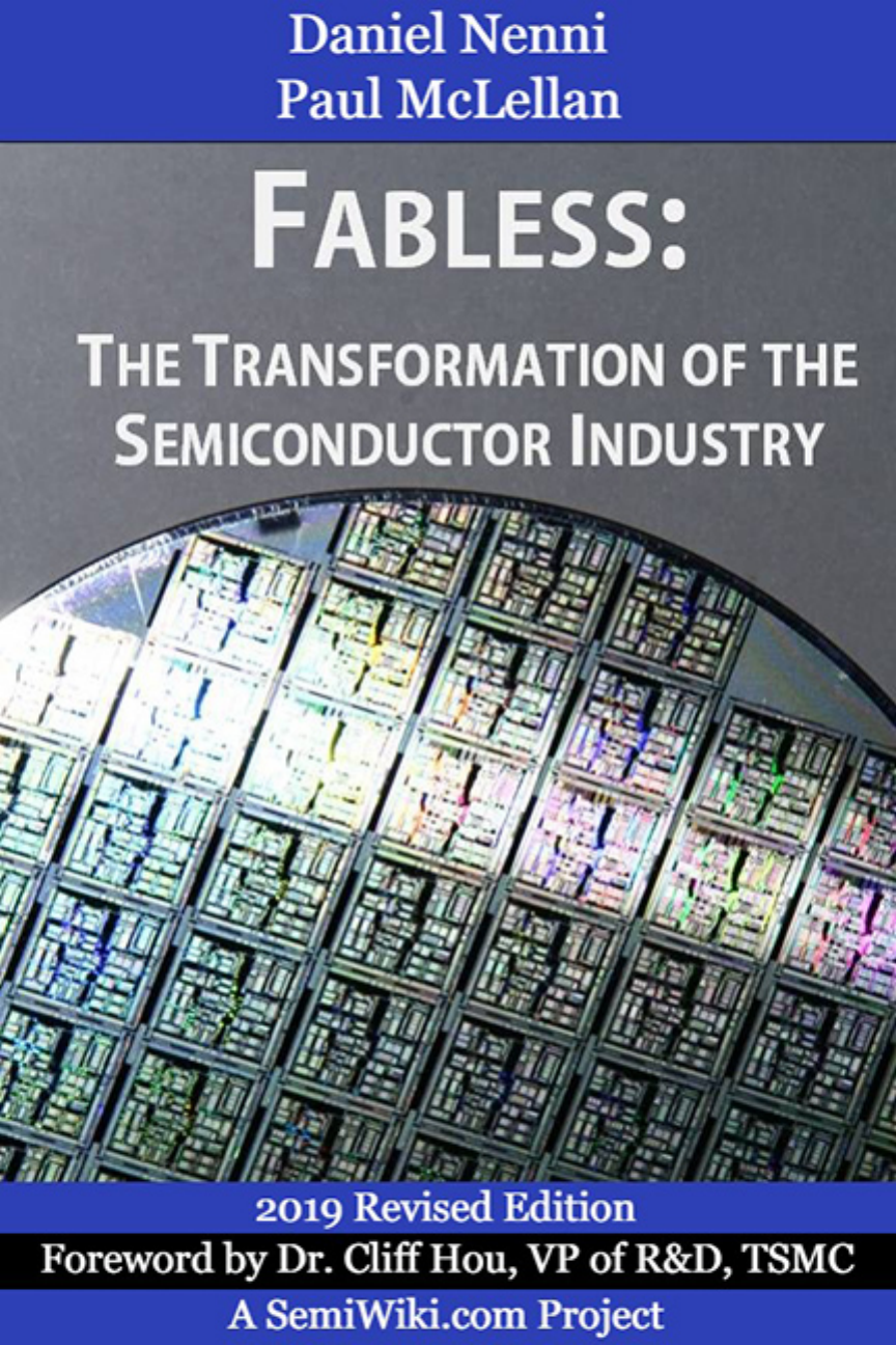
In 1965, Gordon Moore was the head of research and development at
Fairchild. Moore noticed that the number of transistors on the integrated
circuits that Fairchild was building seemed to double every two years, as
shown in the graph from Moore’s original 1965 article in Electronics (vol.
38, number 8) titled, “Cramming More Components onto Integrated
Circuits.”
Moore’s original graph. It predicts a steady rise in the number
of transistors on a chip.
As he pointed out there, “Integrated circuits will lead to such wonders as
home computers, automatic controls for automobiles, and personal
portable communications equipment.”
Remember that this was 1965, when an integrated circuit contained
64 transistors. This was an extraordinary prediction. And he was right;
we do have home computers, automatic controls for automobiles (not
quite fully automatic yet), and personal portable communications
19
equipment also known as cellphones. His prediction differed from
popular science fiction assumptions about future technology because it
was based on observed facts about the trajectory of computational capacity.
Notice that he did not predict flying cars or unlimited power sources, two
technologies that were assumed to be inevitable by mid-century futurists.
Surprisingly, nearly 50 years after Moore made his observation,
semiconductors seem still to be increasing in complexity at this rate.
Gordon Moore’s original prediction is now known as “Moore’s Law.”
However, it is possible to look at Moore’s Law another way: the cost of
any given functionality implemented in electronics halves every two years
or so. Over a period of twenty years, this is a thousand-fold reduction. A
modern video-game console has far more computing power and much
better graphics than the highest-end flight simulators of the 1970s. Every
ink-jet printer has far more computing power than NASA had at its
disposal for getting to the moon.
It is this exponential reduction of electronic costs that has transformed
so many aspects of our lives in the last twenty years or so since integrated
circuits became cheap enough to go into consumer electronic products.
Because of this fast growth in semiconductor technology, we have certain
expectations about electronics that we don’t have for anything else. We
don’t expect our cars to cost half as much or get double the gas-mileage
every few years. Intel made another comparison: if the airline industry
obeyed Moore’s law, a flight from New York to Paris taking seven hours
and costing $900 in 1978 would have taken a second and cost a penny in
2005.
How ICs are Made
The process of designing and manufacturing an IC can seem abstract. In
fact it is complex, but not unfathomable. The design of ICs used to be a
manual task, but is accomplished now with the help of specialized software.
That aspect will be covered later. The basic manufacturing technique has
evolved from the original planar process, in which ICs are built up in layers
20
on top of a disc of silicon called a wafer. A modern wafer is 12” in diameter
(300 mm) with an area of roughly 70,000 sq. mm, about the size of a dinner
plate. If the ICs are small, say 1 mm on each side, the wafer will hold 70,000
of them. If you’re making giant ICs, say 20x20 mm, you can fit only 148 on
a wafer. The ICs on a wafer are called die. Die is used as both singular and
plural in the semiconductor industry.
Starting with the bare silicon wafer, layers of different materials—
semiconductor, metal, and dielectrics—are deposited one at a time. The
layers that define the transistors are created first, then all the transistors are
created. Next, the layers of metal are deposited and then etched with
chemicals to define them into the wires that hook all the transistors
together and to supply power from outside the chip (from the battery in
your cellphone, for example).
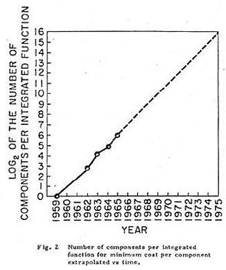
Light shines through a reticle, which acts as a stencil to create
patterns on the wafer. Illustration courtesy of Intel.
The key feature of the production process is that all the transistors on all
the die on the wafer are created simultaneously, and each layer of metal is
created simultaneously across the whole wafer. It is this incredible level of
21
efficiency, making trillions of transistors at once, that has allowed the price
of electronic products to fall by around 5% per month, year after year.
The manufacturing process is based on a photographic process known
as photolithography in which each die is exposed to light through a mask
(more correctly called a reticle). The reticles are usually the negative image
of all the components of the integrated circuit. A machine called a stepper
exposes each die one at a time to a flash of light from a laser through the
reticle, and then steps over to the next die until the whole wafer has been
exposed. The photographic process captures the mask pattern on
photoresist, a wafer coating whose chemical properties are modified by
exposure to the light source through the reticle. The wafer is then
developed, resulting in the corresponding reticle pattern in photoresist at
each die location.
The huge gain in efficiency comes after the stepper is done stamping the
pattern onto each die. That’s when the entire wafer is processed (etched,
doped, heated, etc.) to transform the patterns into the real transistors, wires,
and vias that connect the metal on different layers that make up the final
integrated circuit.
It is worth emphasizing that the manufacturing process doesn’t depend
on what is being manufactured. A computer printer doesn’t need to be
reconfigured depending on what you want to print, you just send it
different data. In the same way, a semiconductor manufacturing process
doesn’t depend on what the circuit is going to do.
The full details of the manufacturing process are obviously too complex to
go into here. The important thing to remember is that it doesn’t matter how
many transistors are on the die, or what the final product will be— all
transistors on a die are created at once and all die on the wafer are processed
very efficiently at the same time.
Where ICs are Made
The factories that make ICs are called fabs. Inside the fab is kept very
clean—a hospital operating theater is filthy by the standards of the “clean
22
rooms” in a fab. The air in the fab may be completely changed every few
seconds, as high-efficiency particulate air (HEPA) filters in the ceiling blow
air down and out through perforations in the floor before being filtered
and recirculated. In fact, recently, fabs have found that even that air is not
clean enough. Even a few random particles landing on a die can ruin it.
These days, the wafers being processed are contained in even cleaner boxes
that attach to each piece of manufacturing equipment in turn. A large part
of the cost of a fab is not the manufacturing equipment, expensive though
it is, but the equipment for keeping everything inside the fab clean.
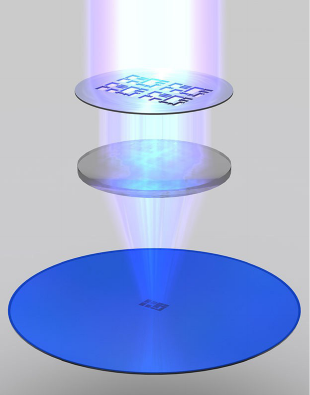
Inside an Intel fab, a technician works in a clean suit, or
“bunny suit.” Image courtesy of Intel.
Why is cleanliness so important? The transistors on a modern
integrated circuit are 20 nanometers (nm) across. There are 1 million
nanometers in a millimeter. By contrast, a human hair is around 100,000
nm. Obviously, a hair ending up on a wafer would be a complete disaster,
blocking thousands of transistors from being manufactured correctly
and causing that die to fail. But it only takes something around 10 nm across
to fall on the wafer to cause a die to (probably) fail. If a die is not
manufactured correctly, it is simply thrown away. There is typically no
repair process to fix it after it’s made.
A modern fab is wildly expensive. One major company estimated a cost
of $10 billion dollars for the fab due to start construction in 2014. Since it
23
has a lifetime of perhaps 5 years, owning a fab costs around $50 per second,
and that’s before you buy any silicon or chemicals or design any chips.
Obviously, anyone owning a fab had better plan on making and selling a
lot of chips if they are going to make any money. That’s exactly what they
do: a modern fab manufactures over 50,000 dinner-plate sized wafers every
month.
Fabs were not always so expensive and until relatively recently, most
semiconductor companies owned their own fabs. In 1980 there were no
semiconductor companies that didn’t own their own fabs to manufacture
their own designs. However, the economics of fabs has completely changed
the semiconductor ecosystem over the last twenty years or so.
The model for semiconductor companies now is to outsource
manufacturing. Companies that do this are called ‘fabless’ and the
companies that manufacture their ICs are called foundries. This change in
the semiconductor ecosystem is a recurring theme of this book and has
been essential to the success of the semiconductor industry.
Business Models from Fab to Fabless
The first step that led to the outsourcing of manufacturing was when
companies began sharing their in-house fabs with other companies. A
company with a large fab would have excess capacity at times. To keep the
lines busy, they sold that capacity to other companies who needed more.
Then, in the early 1980s, a new type of semiconductor company formed
that specialized in helping systems companies design just the right chip for
their application, as opposed to buying standard ICs off the shelf. These
new companies would supply the knowledge of physical chip design and
also manufacture the chips (or have them manufactured) and ship them
back to the systems companies. These chips were known as application
specific integrated circuits or ASICs (although the less catchy term
“customer specific integrated circuits” would have been more accurate).
The ASIC model allowed companies to design custom integrated circuits
without having to maintain the infrastructure of a fab.
24
By the mid-1980s, more companies started making specialized ICs, but
without investing in their own fabs. Instead, these companies would
purchase excess foundry capacity from other fabs. These companies came
to be called, for obvious reasons, fabless semiconductor companies. This
was when semiconductor companies with fabs became known as IDMs
(integrated device manufacturer), to distinguish them from the fabless
companies.
In 1987, another new breed of semiconductor company was created: the
pure-play foundry. A pure-play foundry only manufactures ICs for other
companies who are either fabless or had limited capacity in their own fabs.
They do not design semiconductor products themselves. Before the foundry
business came along, getting a semiconductor company off the ground
was difficult and expensive. Building a fab was expensive, and starting a
fabless semiconductor company required a complicated negotiation for
excess foundry capacity at a friendly IDM. Once foundries arrived, the cost
and the risk of entering the semiconductor market lowered drastically. The
result? A surge of new fabless semiconductor companies in the 1990s, many
funded by Silicon Valley venture capitalists to address the growing markets
for computer graphics, networking chips, and wireless phone chips.
The move to a fabless model wasn’t universally hailed as a good idea. Jerry
Sanders, the co-founder and long-time CEO of Advanced Micro Devices
(AMD), famously noted in the late 1980s as the fabless revolution was getting
underway, that, “Real men have fabs.” What he meant was that design and
process needed to be tightly coupled. Because AMD was competing with
Intel in the microprocessor business, this statement was possibly true for
his business. It turned out not to be true for many businesses.
Over time, another change happened. As the specialized knowledge
about how to design integrated circuits gradually spread, many systems
companies stopped using the ASIC companies in favor of doing their
designs in-house. By the 1990s, many systems companies had very large
integrated circuit design teams and the ASIC companies gradually started
25
selling more and more of their own products until they became, in effect,
IDMs.
As fabs got more expensive, more IDMs (like Texas Instruments and
AMD) also chose the fabless model. Some switched to being completely
fabless, others kept their own older fabs and used the third-party foundry
for the most advanced ICs. This was known as fab-lite.
This is the landscape today. There are a few IDMs such as Intel who
design almost all of their own chips and build them in their own fabs. There
are foundries who design no chips, they only manufacture them for other
companies. Then there are fabless semiconductor companies such as Xilinx
and Qualcomm along with their fab-lite brethren such as Texas
Instruments, who design their own chips, sell their own products, but use
foundries for all or part of their manufacturing.
Along the way, there have been other players that helped bring
semiconductor technology and business to the current state. One is called
electronic design automation (EDA), which is the specialized software that’s
needed to design ICs. This software was once developed in house by each
semiconductor company, but was later outsourced. The same is true for the
components that go onto many ICs, or systems-on-chips (SoCs).
Semiconductor companies once had to make all the components that went
on their chips themselves, or have them custom made by another company.
Now there is a robust market for licensing a wide variety of off-the-shelf
functions to put on chips. These include things like A/D converters,
memory, and processors, and are collectively known as silicon intellectual
property, or IP.
From the IC to the iPad
With this basic history of the transistor, we can look at the changes in the
semiconductor business and technology through the years and see how
we’ve arrived at the current state of the industry. The chapters of this book
cover the main story arc of the semiconductor industry:
26
• Genesis: the invention of the transistor and the integrated circuit
• The first major transition from off-the-shelf components to
ASICs
• The second major transition from owning fabs to the fabless model
• The growth of EDA: selling the software that makes it all work
• The role of IP: selling the building blocks for chips
• The future: industry luminaries look to what comes next
Each main topic is presented in a chapter that explores the history and
key technologies. Each chapter is punctuated by sections that were
contributed by the leading companies in the fabless semiconductor
landscape today. They explain in their own words their history and role in
the larger ecosystem. The last chapter of the book passages from industry
luminaries who share their vision of what will take the semiconductor
industry to the next level of innovation and financial success. Our hope is
that this combination of objective and subjective histories is both
informative and entertaining.
27
Chapter 2: The ASIC Business
Before the 1980s, ICs contained a limited number of transistors and were
designed and created by the traditional semiconductor companies like
Fairchild and Texas Instruments. The chips were generic; basic building
blocks that everyone bought and made into products. However, by the
early 1980s, as semiconductor technology reached a point where much
more functionality could be fit onto a single chip, the people who made
electronics products began to search for new ways to stand out from the
competition. They wanted ICs that were differentiated from the
competition, and that were tuned to work specifically in their products.
This drove the development of a new type of chip, the application-specific
integrated circuit or ASIC, and a new business model that drastically
changed the layout of the semiconductor industry.
Traditional Semiconductor Business Stalls
The business model of semiconductor companies from the beginning of
the IC until the 1980s was to imagine what the market needed, create it,
manufacture it and then sell it on the open market to multiple customers.
As electronic products became more sophisticated, their customers wanted
chips that more specifically met their needs, rather than the generic chips that
were available to everyone. This was something the traditional
semiconductor companies were not equipped to provide for both business
and technical reasons. On the technical end, semiconductor companies
knew a lot about semiconductors, but they lacked system knowledge, and
28
so were unable to design specific ICs for every market segment. On the
business side, providing more versions of their products would increase
design overhead costs and reduce the advantages of manufacturing huge
volumes of a limited number of products. The systems companies, on the
other hand, knew exactly what they wanted to build but didn’t have enough
semiconductor knowledge to create their own chips and didn’t have the
means to manufacture those chips even if they could design them. The
systems companies needed a new way of doing chip design.
The ASIC Business Blooms
There was clearly a new niche forming for a business that could figure
out how to create custom ICs for systems companies. Two companies in
particular, VLSI Technology and LSI Logic, pioneered this new ASIC
business. They both applied deep knowledge of semiconductor design and
manufacturing to a business model that consisted largely of building other
people’s chips. What emerged was a model in which the systems companies
did the early part of the design (called front-end) that specifies the exact
functionality they want, then handed the physical design (called back-end)
and manufacturing responsibilities to the ASIC company.
While it was initially thought of as a terrible business to be in—high
engineering costs and few customers—the advantages to this new model
became evident and the new ASIC companies did very well. LSI Logic, for
example, reported revenues of $2.75 billion by 2000.
The new ASIC model set the stage for a cascade of changes to the
semiconductor industry. For example, the budding electronic design
automation companies took note of this new market. They realized that
their design automation systems used for printed circuit boards could also
be used for the front-end steps of ASIC design too.
How the ASIC Design Model Works
ASIC design typically worked like this: A systems company, typically one
building an add-on board for the PC market that was the big driver of
29
electronics in that era, would come up with some idea for a new chip. They
would negotiate with several ASIC companies and choose one to work with
even though they only had a vague idea of the size of the design at that
point. The chosen ASIC company would supply them with a library of basic
building blocks called standard cells.
The systems company would use a software tool called a schematic editor
to create the design, picking the cells they wanted from the library and
deciding how those cells should be connected. The output from this
process is called a netlist, essentially a list of cells and connections.
Just like writing software or writing a book, the first draft of the design
would be full of errors. But with semiconductor technology, it isn’t possible
to build the part and see what the errors are. Even back then,
manufacturing the first chip, known as the prototype, could cost tens of
thousands of dollars and take a couple of months. Also unlike book writing,
it’s not possible to simply proofread or inspect the schematic; too many
errors would still slip through.
Instead, designers simulated the function of the design with software. A
flight simulator tells a pilot what would happen if he or she moves the
controls a certain way, and there is no cost to crashing in the simulation. In
the same way, a simulation of the design checked how it behaved given
certain inputs without requiring the expense of building the chip. Errors
detected through simulation could be fixed and the simulation could be run
again until no more errors remained.
When the design was finally determined to be functionally correct, the
netlist was sent from the systems company to the ASIC company for the
next step. Using a software program that placed the standard cells and
wired them together (known as place & route), the netlist would be
converted to a physical layout. The netlist is a list of cells and connections,
something like an architectural spec that says which room connects to
which and by how many doors; the output of place & route adds the
30
physical locations and specific wire routing, analogous to a completed
house blueprint.
In addition to creating the actual layout that will be manufactured, this
process also created a detailed account of timing—how long every signal
takes as it travels from its source to the transistor it switches on or off. This
detailed timing was sent back to the systems company for a final simulation
to ensure that everything still worked.
After the design passed final simulation, the systems company took a
deep breath and gave the go-ahead to manufacture prototypes of the chip. At
the time, all the design data needed to make the photomask was written onto
a computer tape, so the process was, and still is, called tape-out.
The ASIC company then had the masks made that were needed to run
the design through their fab. Chips were manufactured using one of two
main ASIC technologies; gate-array or cell-based. In a gate-array design, the
gates—a group of transistors that perform a function—were pre-fabricated
on a wafer (the gate-array “base”) so the masks only pattern the
interconnect. In cell-based design, masks were required to pattern all layers
on a blank wafer. The gate-array approach was faster and cheaper, but less
flexible. It was faster, because there were fewer masks to make and fewer
layers to be manufactured. It was cheaper, because the gate-array bases
were mass produced in higher volume than any individual design would be.
However, gate-array substrates only came in certain fixed sizes, and so the
designs often left many potential gates unused.
In a couple of months, the prototypes would be finished and samples
shipped back to the systems company. These parts would then be
incorporated into complete systems and those systems tested. For example,
if the chip went into an add-in board for a PC, a few boards would then be
manufactured, put into a PC, and checked for correct operation.
At the end of that process, the systems company took another deep
breath and placed an order with the ASIC company for volume
manufacturing; requesting thousands, or possibly even millions, of chips.
31
They would receive these a few months later, build them into their own
products, and ship those products to market. The final step in this journey
was the day we, the consumers, brought home our very own personal
computer or CD player.
The Lasting Effect of the ASIC Model
All semiconductor companies were caught up in ASIC in some way or
another because of the basic economics. Semiconductor technology
allowed systems companies to make medium-sized designs, and medium-
sized designs were pretty much all different. The technology didn’t yet
allow whole systems to be put on a single chip. This meant that
semiconductor companies could no longer survive by just supplying basic
building-block chips because those were largely being superseded by ASIC
chips. But they also couldn’t build whole systems like a PC, a television, or
a CD player because semiconductor technology did not allow for that level
of integration. Eventually, most semiconductor companies, including
Panasonic, Fujitsu, and Intel, joined the ASIC business, thus making the
market very competitive.
Although the ASIC business model filled an important niche in the
development of electronic products, it turned out to be a difficult business in
which to make money. The systems company owned the specialized
knowledge of what was in the chip, so the semiconductor company could
not price to value. The systems company also knew the size of the chip and
thus roughly what it should cost to make. The best money for ASIC
companies turned out to be making the largest, most difficult designs. It
took more expertise to successfully complete the physical design of these
big designs, so the leading ASIC companies, VLSI Technology and LSI
Logic, could charge premium pricing based on their ability to complete the
most challenging designs on schedule. If you are building a sky-scraper you
don’t go with a company that has only built houses.
ASIC companies had few designs they could make money on, and it
gradually became obvious just how unprofitable low-volume designs were.
32
All the ASIC companies realized that there were less than a hundred
designs a year that were really worth winning, and competition to win those
became fierce.
During this time, semiconductor technology continued to advance and it
became possible to build whole systems (or large parts of them) on a single
integrated circuit. These were known as systems-on-chip, or SoCs. The
ASIC companies started to build and sell whole systems, such as chipsets
for PCs or cellphones much like the traditional semiconductor model,
alongside their traditional ASIC business. This made all semiconductor
companies start to look the same, with lines of standard products and,
often, an ASIC product line too.
One important aspect of the ASIC model was that the “tooling,” the
industry word for the photomasks, belonged to the ASIC company. This
meant that any given design could only be manufactured by its specific
ASIC company. Even if another semiconductor company offered them a
great deal to manufacture a completed design, the systems company
couldn’t just hand over the masks made by a previous ASIC company. This
became very important in the next phase of what ASIC would morph into:
design services.
ASIC design required a network of design centers all over the world
staffed with some of the best designers available, obviously an expensive
proposition. Their customers started to resent paying the premium to
support this infrastructure, especially on very high volume designs. While
the systems companies could shop around for a better price, switching
vendors was costly because it meant starting the design all over again with
the new semiconductor supplier.
Eventually both VLSI Technology and LSI Logic would be acquired.
VLSI was bought by NXP (still then called Philips Semiconductors) in 1999
for close to $1 billion. LSI Logic, which left the ASIC business and was
renamed LSI Corporation, was acquired by Avago in late 2013 for $6.6
billion.
33
The ASIC Model Morphs into Design Services
By the early 1990s, in addition to the high cost of the ASIC model, two
other things had changed that spelled the beginning of the end for the ASIC
business. One was that foundries such as TSMC had come into existence.
The second is that the knowledge of how to do physical design became
more widespread and at least partially encapsulated in software tools
available from the EDA industry. These changes gave systems companies
a new route to silicon that bypassed the ASIC companies completely.
Systems companies could now feasibly complete the entire design
themselves, including the physical design, and then use a foundry like
TSMC to manufacture it. This was known as customer-owned-tooling or
COT, because the systems company, not the ASIC company or the foundry,
owned the whole design from concept to masks. If one foundry gave poor
pricing, the systems company could transfer the design to a different
manufacturer without having to completely redesign the chip.
However, the COT approach was not without its challenges. Doing
physical design of a chip is not a simple task. Many systems companies
underestimated the value of the premium charged by ASIC companies for
their expertise, and they struggled to complete designs on their own
without that support. As a result, a new breed of companies, known as
design services companies, emerged to meet this exploding demand for
support.
Design service companies played a similar role as the ASIC companies;
providing specialized semiconductor design knowledge to the systems
companies. In some cases, they would do the entire design, which is called
turn-key design. More often, they would do all or some of the physical
design and sometimes manage the interface with the foundry to oversee
the manufacturing process, another area where systems companies lacked
experience. One company in particular, Global Unichip, operates with a
business model identical to the old ASIC companies except in one
respect—it has no fab. It uses a foundry, primarily TSMC, to build all of
their customers’ products.
34
This is the layout of the ASIC landscape today: there is very limited ASIC
business conducted by a few semiconductor companies. There are design
services companies and virtual ASIC companies like Global Unichip and
eSilicon. There are no pure-play ASIC companies. A lot of IC functions
that were once implemented as ASIC are now mostly done as field-
programmable gate arrays, or FPGA, which is important enough to need a
chapter of its own. The next main chapter, in fact, is an exploration of
FPGAs. But first, a brief history of one of the companies that created the
ASIC business model, VLSI Technology, and one of the new breed of
design services companies, eSilicon.

35
In Their Own Words: VLSI
Technology
As one of the companies that founded the ASIC business
model, VLSI Technology helped set the course of the entire
semiconductor industry. The company is no longer in business,
but one of their early and long-time employees, and co-author
of this book Paul McLellan, has written this history of
VLSI Technology.
VLSI Technology was founded in 1979 by Dan Floyd, Jack Baletto and
Gunnar Wetlesen, who had worked together at the semiconductor
company Signetics. The initial investments in VLSI Technology were from
Hambrecht and Quist, a cross between a VC and a bank, and by Evans and
Sutherland, the simulation/graphics company. Semiconductor technology
had reached a point that significant systems or parts of systems could be
manufactured, and the original business plan was to build a fab to
manufacture parts that other people would design.
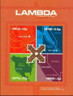
The fourth person to join the company, in 1980,
was Doug Fairbairn. He was working at Xerox Palo
Alto Research Center (PARC) and had started a fledgling publication on
very-large-scale integration (VLSI) design, Lambda Magazine. He went to
interview the three founders for an article, but was intrigued by the new
company.
36
He immediately realized that their plans for a foundry wouldn’t really
work without a new generation of design automation tools. Existing design
tools of that era were polygon-based layout editors, but semiconductor
technology was already past the point where you could reasonably design
everything by hand. Doug decided to take the opportunity to move from
the research environment into industry and create the first development
group creating the next generation of software for integrated circuit design.
In the first few years of VLSI Technology, the company was sustained
by designing ROMs (read-only memories) for the first generation of video
game consoles, which were all cartridge-based. Each cartridge actually
contained a ROM with the video-game binary programmed into it. The fab
in San Jose was not yet in high volume manufacturing, and so these were
actually outsourced to Rohm in Osaka, Japan. In parallel, Fairbairn hired a
group of PhDs, many from Carver Mead’s Silicon Structures Project at
CalTech, and the profits from video games were invested in a suite of tools
for what we would now call ASIC design, although that name didn’t come
until later.
Lambda Magazine.
VLSI Technology (hereafter simply VLSI) had a fab on McKay Drive in
San Jose. At the time, it was the only high-tech building in the area,
surrounded by greenhouses growing flowers and, across the street, the
37
Chrysanthemum Growers Association Hall that was sometimes used for
company-wide meetings. The first process brought up was 3 µm HMOS,
followed by 2 µm CMOS and 1.5 µm CMOS.
Fairly early on, the investors decided that the company’s management
team was too inexperienced to manage the anticipated growth. Al Stein was
brought in as CEO. The company went public in February 1983, still not
yet profitable, and almost immediately afterward, the three original
founders departed.
The initial design technology still based largely on the Caltech/PARC
ideas in Mead and Conway’s seminal book, Introduction to VLSI Design, was
a mixture of manual design with generators for basic structures, such as
registers and adders, using an internal language called VIP. The focus of the
tools was on verification, with a design rule checker (DRC), a circuit
extractor, a layout-versus-schematic (LVS) checker, called net compare, and
simulators—VSIM, with no timing and then TSIM, which had timing-based
on a simple capacitive model.
However, designs were getting too large for this approach and despite
the inelegance compared to Mead and Conway’s ideas, it was clear that
layout tasks had to become much more automated. This fact led them to
develop standard cell libraries and a full place and route system to
complement their existing schematic capture software.
In order to be successful, the design work had to get closer to the
customer. Initially this meant that the customer came to VLSI, and there
were several teams of customer’s designers working on site at VLSI’s San
Jose buildings. For example, the main chip in France Telecom’s initial
implementation of the online service, Minitel, was created by Telic (now
buried somewhere in Alcatel-Lucent) who sent a team of engineers from
Strasburg, Germany to San Jose who took up residence for several months.
The next step was to create a network of design centers initially in the
US, and then also in Japan and Europe, since it was clearly not scalable to
bring all the customers on-site to California.
38
VLSI also opened a research and development site at Sophia Antipolis in
the south of France. They started doing design tool development and
library development, and also served as a hub of expertise to support the
growing European business.
The IBM PC was then in its high growth phase and many customers of
VLSI were designing products for that market (modems, add-in peripheral
cards) or designing chips to create PC clones. In fact, VLSI had dozens of
customers making products for the PC market. To serve these customers,
VLSI developed the first of what today is called semiconductor IP,
although VLSI called them megacells (and later functional system blocks
or FSBs). These included all the standard components in a PC such as the
UARTs or the 6845 graphics controller.
Two key design automation products that VLSI pioneered in the late
1980s were the datapath compiler and the state-machine compiler, which
was effectively one of the first synthesis tools. The datapath compiler could
take a complex description for a datapath and quickly generate a fully laid
out datapath on silicon, using its own optimized custom library, not
standard cells. And the state-machine compiler could take a description of
a state machine (or just any old logic) and produce an optimized
implementation in standard cells. Together these two tools made creating
complex designs much easier.
VLSI saw robust growth in the 1980s, but it never made enough cash to
fund all the investment required for process technology development and
capital investment for a next-generation fab. They also had several false
starts. They entered and then exited the SRAM (static memory) business.
They entered and then exited a partnership to build a fab in Malaysia. They
had a partnership with Philips Semiconductors licensing process
technology that was never used.
In the late 1980s, they entered into a strategic partnership with Hitachi
in which Hitachi gained access to VLSI’s design tools and Hitachi licensed
VLSI its 1 µm process technology and made significant cash investment.
39
This meant that VLSI could bring up a competitive 1 µm technology at its
second fab in San Antonio, TX. Eventually the two fabs were upgraded
from 5” to 8” wafers.
Development of the Chip Set
VLSI had already developed several megacells as IP for use in PCs. A
group of five engineers conducted an experiment with these megacells over
a weekend that involved putting all of them together onto a few chips. This
was the first PC chipset, which could be used to create a full PC with only
the addition of the Intel microprocessor and memory. VLSI ran with the
idea and built up a large business in PC chipset standard products to go
with its mainline ASIC business.
The PC chipset business was very successful and was dominated by VLSI
in the early 1990s. One generation of chipsets was even resold by Intel.
However it was clear that it would eventually become a low-margin business
due to competition from Asia, and probably would finally be owned by
Intel who could design more and more functionality to work intimately with
its own next-generation microprocessors. VLSI decided to invest in system
knowledge for the GSM cellular standard that was starting to get off the
ground, as well as some other attractive end markets such as digital video.
Also, in that era, around 1987, Apple decided to build the Newton
personal digital assistant. They selected Acorn’s RISC processor and
insisted it be spun out as a separate company. So, ARM was created with
Apple, Olivetti (that by then owned Acorn) and VLSI as the owners. VLSI
supplied all the design tools used to design the processors, and also
manufactured the initial parts. That story is told in more detail later in the
book.
Meanwhile, the market for second generation (digital) GSM phones
exploded. European companies, especially Nokia and Ericsson, were the
most successful handset manufacturers. At one point Ericsson was
accounted for 40% of VLSI’s entire business. VLSI also started a major
investment at its French site to develop its own GSM baseband chips. They
40
built this up into a chipset business selling to second-tier manufacturers
who didn’t have enough system knowledge to develop GSM baseband
chips internally. They later licensed CDMA wireless technology from
Qualcomm and started to develop a CDMA product line primarily for the
US market. Between the standard product business and the large volume
of ASIC business, especially with Ericsson, the communication segment was
over half of VLSI’s semiconductor business.
By 1991, it was clear that VLSI was really two companies that should
already have separated: an EDA company with some of the best VLSI
design tools on the market, and an ASIC/ASSP company with a network
of design centers and two fabs manufacturing silicon. In 1991, the design
tool business was spun out to a new company called Compass Design
Automation, leaving VLSI Technology as a pure semiconductor business
(with Compass as one of their EDA suppliers).
Compass struggled to shake off the perception that it wasn’t really
independent of VLSI and as a result it had only a small ecosystem of
semiconductor companies that fully supported it with ASIC libraries. But
Compass also had its own portfolio of libraries, originally developed for
VLSI’s ASIC business. By creating standardized design rules (called
Passport) that worked in almost all fabs, it created the first library business
with a portfolio of standard cells, memory compilers, the datapath
compiler, and other foundation IP. This was very successful and grew to be
about 30% of Compass’s business.
Compass increased to nearly $60 million in revenue but it was never
profitable. They had a fully integrated suite of design tools in an era when
the large EDA companies, which had grown through acquisition, had
educated the market to pick best-in-class point tools and use their internal
CAD departments to integrate them. So Compass was swimming against
the tide and despite the fact that every ASIC and every standard product
made by VSLI was designed exclusively using Compass tools and libraries,
they never shook off the perception that they were not leading edge. CAD
41
groups were reluctant to standardize on Compass, at least partially because
they would have much less design tool integrating to do.
In 1997, Compass was sold for $44 million to Avant!, which was mostly
interested in the library business to complement their own software
business. Of course, Avant! in turn was acquired by Synopsys in 2001 (for
$830 million). The software part of the business, as opposed to the library
development, by then was largely based in France and the entire group in
France was hired by Cadence en-masse where many of the individual
engineers still work today. The library business was largely in California and
was integrated into Avant!
VLSI’s semiconductor business, both the ASIC business and the ASSP
business grew through the 1990s to about $600 million in revenue. There
was a focus on wireless, digital video, PC graphics and an ASIC business
that was diversified into many separate segments.
In 1999, Philips Semiconductors (now called NXP) made a hostile
takeover bid for VLSI Technology. Philips had struggled to bring processes
to market quickly along with the required libraries. As the ASIC business
got more and more consumer-oriented, this became a big problem because
of the very short product life-cycles. VLSI’s lifeblood was ASIC and they
were much quicker at getting designs going in new process generations, so
Philips figured that acquiring VLSI would shake up their internal processes
and also give them a network of leading design centers (by then renamed
technology centers). After some negotiation, VLSI was acquired by Philips
Semiconductors for just under a billion dollars and it ceased to be an
independent company.
43
In Their Own Words: eSilicon
Corporation
eSilicon was one of the first companies to focus on making
the benefits of the fabless semiconductor movement available
to a broader range of customers and markets. The company
is credited with the creation of the fabless ASIC model. In
this section, eSilicon shares some of its history and provides
its view of the ever-changing fabless business model.
eSilicon Corporation was founded in 2000 with Jack Harding as the
founding CEO and Seth Neiman of Crosspoint Venture Partners as the
first venture investor and outside board member. They both remain
involved in the company today, with Harding continuing as CEO and
Neiman now serving as Chairman of the Board.
Both Harding and Neiman brought important and complementary skills
to eSilicon that helped the company maneuver through some very
challenging times. Prior to eSilicon, Harding was President and CEO of
Cadence Design Systems, at the time the largest EDA supplier in the
industry. He assumed the leadership role at Cadence after its acquisition of
Cooper and Chyan Technology (CCT), where Harding was CEO. Prior to
CCT, Harding served as Executive Vice President of Zycad Corporation, a
specialty EDA hardware supplier. He began his career at IBM.
Seth Neiman is Co-Managing Partner at Crosspoint Venture Partners,
where he has been an active investor since 1994. Neiman’s investments
include Brocade, Foundry, Juniper and Avanex among many others. Prior
44
to joining Crosspoint, Neiman was an engineering and strategic product
executive at a number of successful startups including Dahlgren Control
Systems, Coactive Computing, and the TOPS division of Sun
Microsystems. Neiman was the lead investor in eSilicon and incubated the
company with Jack at the dawn of the Pleistocene epoch.
The Early Years
eSilicon’s original vision was to develop an online environment where
members of the globally disaggregated fabless semiconductor supply chain
could collaborate with end customers looking to re-aggregate their services.
The idea was straight-forward—bring semiconductor suppliers and
consumers together and use the global reach of the Internet to facilitate a
marketplace where consumers could configure a supply chain online. The
resultant offering would simplify access to complex technology and reduce
the risk associated with complex design decisions. Many fabless enterprises
had struggled with these issues, taking weeks to months to develop a
complete plan for the implementation of a new custom chip. Chip die size
and cost estimates were difficult to develop, technology choices were varied
and somewhat confusing, and contractual commitments from supply chain
members took many iterations and often required a team of lawyers to
complete.
The original vision was simple, elegant and sorely needed. However, it
proved to be anything but simple to implement. In the very early days of
the company’s existence, two things happened that caused a shift in
strategy. First, a close look at the technical solutions required to create a
truly automated marketplace yielded significant challenges. Soon after the
formation of the company, eSilicon hired a group of very talented
individuals who did their original research and development work at Bell
Labs. This team had broad knowledge of all aspects of semiconductor
design. It was this team’s detailed analysis that lead to a better
understanding of the challenges that were ahead.
45
Second, a worldwide collapse of the Internet economy occurred soon
after the company was founded. The “bursting” of the Internet bubble
created substantial chaos for many companies. For eSilicon, it meant that a
reliable way to monetize its vision would be challenging, even if the
company could solve the substantial technical issues it faced. As a result,
most of the original vision was put on the shelf. The complete realization
of the “e” in eSilicon would have to wait for another day. All was not lost
in the transition, however. Business process automation and worldwide
supply chain relationships did foster the development of a unique
information backbone that the company leverages even today. More on
that later.
The Fabless ASIC Model
Mounting technical challenges and an economic collapse of the target
market have killed many companies. Things didn’t turn out that way at
eSilicon. Thanks to a very strong early team, visionary leadership and a little
luck, the company was able to redirect its efforts into a new, mainstream
business model. It was clear from the beginning that re-aggregating the
worldwide semiconductor supply chain was going to require a broad range
of skills. Certainly, design skills would be needed. But back-end
manufacturing knowledge was also going to be critical. Everything from
package design, test program development, early prototype validation,
volume manufacturing ramp, yield optimization, life testing, and failure
analysis would be needed to deliver a complete solution. Relationships with
all the supply chain members would be required and that took a special
kind of person with a special kind of network.
eSilicon assembled all these skill sets. That deep domain expertise and
broad supply chain network allowed the company to pioneer the fabless
ASIC model. The concept was simple—provide the complete, design-to-
manufacturing services provided by the current conventional ASIC
suppliers, such as LSI Logic, but do it by leveraging a global and outsourced
46
supply chain. Customers would no longer be limited to the fab that their
ASIC supplier owned, or their cell libraries and design methodology.
Instead, a supply chain could be configured that optimally served the
customer’s needs. And eSilicon’s design and manufacturing skills and
supply chain network would deliver the final chip. The volume purchasing
leverage that eSilicon would build, coupled with the significant learning
eSilicon would achieve by addressing advanced design and manufacturing
problems on a daily basis would create a best-in-class experience for
eSilicon’s customers.
eSilicon’s positioning, DAC 2000
As the company launched in the fall of 2000, the fabless ASIC segment
of the semiconductor market was born. Gartner/ Dataquest began
coverage of this new and growing business segment. Many new fabless
ASIC companies followed. Antara.net was eSilicon’s first customer. The
company produced a custom chip that would generate real-world network
traffic to allow stress-testing of e-business sites before they went live.
Technology nodes were in the 180 nm to 130 nm range and between
eSilicon’s launch in 2000 and 2004, 37 designs were taped out and over 14
million chips were shipped.
Fabless ASIC was an adequate description for the business model as
everyone knew what an ASIC was, but the description fell short. A
managed outsourced model could be applied to many chip projects, both
standard and custom. As a result, eSilicon coined the term Vertical Service
47
Provider (VSP), and that term was used during the company’s initial public
exposure at the Design Automation Conference (DAC) in 2000.
The model worked. eSilicon achieved a fair amount of notoriety in the
early days as the supplier of the system chip that powered the original iPod
for Apple. The company also provided silicon for 2Wire, a company that
delivered residential Internet gateways and associated services for providers
such as AT&T. But it wasn’t only the delivery of “rock star” silicon that set
the company apart; some of the original e-business vision of eSilicon did
survive.
The company launched a work-in-process (WIP) management and
logistics tracking system dubbed eSilicon Access® during its first few years.
The company received a total of four patents for this technology between
2004 and 2010. eSilicon Access, for the first time, put the worldwide supply
chain on the desktop of all eSilicon’s customers. Using this system, any
customer could determine the status of its orders in the manufacturing
process and receive alerts when the status changed. eSilicon uses this same
technology to automate its internal business operations today.
Growing the Business
During the next phase of growth for the company, from 2005 to 2009,
an additional 135 designs were taped out and an additional 30 million chips
were shipped. Technology nodes now ranged mainly from 90 nm down to
40 nm. It was during this time that the company began expanding beyond US
operations. Through the acquisition of Sycon Design, Inc., the company
established a design center in Bucharest, Romania. A production operations
center was also opened shortly thereafter in Shanghai, China.
Recognizing the growing popularity of outsourcing, eSilicon expanded
the VSP model to include semiconductor manufacturing services (SMS).
SMS allowed fabless chip and OEM companies to transition the
management of existing chip production or the ramp-up and management of
new chip production to eSilicon. The traditional design handoff of the ASIC
model was now expanded to support manufacturing handoff. The benefits
48
of SMS included a reduction in overhead for the customer as well as the
ability to focus more resources on advanced product development.
Extensions such as SMS caused the Vertical Service Provider model to
expand, creating the Value Chain Producer (VCP) model. The Global
Semiconductor Alliance (GSA) recognized the significance of this new
model and elected Jack Harding to their Board to represent the VCP
segment of the fabless industry.
In the years that followed, up to the present day, eSilicon has grown
substantially. The number of tape-outs the company has achieved is now
approaching 300 and the number of chips shipped is on its way to 200
million. The company has also expanded into the semiconductor IP space.
While its worldwide relationships for third-party semiconductor IP are
critical to eSilicon’s success, the company recognized that the ability to
deliver specific, targeted forms of differentiating IP could significantly
improve the customer experience.
eSilicon’s first logo. The squares symbolize the
end product—the chip.
Since so many of today’s advanced chip designs contain substantial
amounts of on-board memory, this is the area that was chosen for eSilicon’s
initial IP focus. The company acquired Silicon Design Solutions, a custom
memory IP provider with operations in Ho Chi Minh City and Da Nang,
Vietnam. This acquisition added 150 engineers to focus on custom memory
solutions for eSilicon’s customers.
As of June 30, 2013, eSilicon employs over 420 full-time people
worldwide, of which over 350 are dedicated to engineering. Headquartered in
San Jose, California, the company maintains operations in New
Providence, New Jersey and Allentown, Pennsylvania; Shanghai, China;
49
Seoul, South Korea; Bucharest, Romania; Singapore and Ho Chi Minh City
and Da Nang, Vietnam. The company’s diverse global customer base
consists of fabless semiconductor companies, integrated device
manufacturers, original equipment manufacturers and wafer foundries.
eSilicon sells through both an internal sales force and a network of
representatives.
The Evolving Model
The eSilicon business model has evolved further. VSP and VCP are now
SDMS (semiconductor design and manufacturing services). Arguably the
longest, but perhaps the most intuitive name. Through the years, Silicon
has allowed a broad range of companies to reap the benefits of the fabless
semiconductor model, many of which couldn’t have done it on their own.
eSilicon’s current logo. The three “S” graphic symbolized the
process and culture—speed, simplicity, and self-confidence.
This ability to bring a worldwide supply chain within reach to smaller
companies gave eSilicon its start, but the model has worked well for eSilicon
beyond these boundaries. Today, eSilicon serves customers that are much
larger than eSilicon itself; customers that could “do what eSilicon does.” In
the early days, the company discounted its chances of winning business at
an enterprise big enough to maintain an “eSilicon inside.”
Time has proven this early thinking to be too limiting. Many of eSilicon’s
customers today can clearly maintain an “eSilicon inside,” but they still rely
on eSilicon to deliver their chips. Why? In two words, opportunity cost. It
has been proven over time that for any enterprise the winning strategy is to
focus on the organization’s core competence and invest in that. All other
50
functions should be outsourced in the most reliable and cost-effective
manner possible. Simply put, eSilicon’s core competency fits in the
outsourcing sweet spot for many, many organizations. This trend has
created new value in the fabless semiconductor sector and facilitated many
new design starts.
What’s Next?
As the fabless model grows, there are new horizons emerging. During its
early days, the vision of using the Internet to facilitate fabless technology
access and reduce risk was largely put on the shelf. The reasons included
the challenges of solving complex design and manufacturing problems and
the lack of a clear delivery mechanism over the Web.
Today, these parameters are changing. The Internet is now an accepted
delivery vehicle for a wide array of complex business-to-business solutions.
eSilicon’s talented engineering team has also developed a substantial cloud-
enabled environment that is used to automate its internal design and
manufacturing operations every day. This team consists of many of the
same people who highlighted the challenges of addressing these issues in
the company’s early years. What a difference a decade can make.
What if that automated environment could be made available to end
users in a simple, intuitive way? New work at eSilicon is taking the company
in this direction. The recent announcement of an easy-to-use multi-project
wafer quote system is an example. What once could take two weeks or more,
consisting of many inquiries and legal agreement reviews, is now done in as
little as five minutes with an extension to eSilicon Access. With availability on
both the customer’s desktop and smartphone, this is clearly the beginning
of a new path. eSilicon changed the landscape of fabless semiconductor in
2000 with the introduction of the fabless ASIC model. It’s time to do it
again and bring back the “e” in eSilicon.
51
2019 Update: eSilicon Corporation
A lot has happened since 2013. Some “ups”, some “downs”, a lot of
innovation and some surprises as well. The story told here applies to the
industry in general, not just eSilicon.
We ended the original chapter on eSilicon talking about the potential to
put the “e” back in eSilicon, leveraging an internet-based business model.
That did indeed happen, but there’s so much more to the story.
In our previous closing remarks, we talked about an easy-to-use multi-
project wafer (MPW) quoting system. By way of explanation, an MPW is
essentially a cost-sharing strategy. Rather than one customer paying the full
cost of a mask set and prototype manufacturing run, what if the mask could
contain designs from many customers? Each customer would then get a
pre-determined number of chips from the prototype run and the cost
would be split among all participants. This strategy dramatically reduces the
cost of building a prototype of a new silicon idea.
Our online MPW quoting system held the promise of collapsing a two-
week fact-finding mission into a five-minute, fill-in-the-blanks quote
generation experience. We did deliver that experience, and a lot more. It is
interesting to note that, while the semiconductor industry essentially
created the internet, the people who work in the semiconductor industry
aren’t all that interested in using the internet for their business.
Our online MPW quoting system met with lackluster interest. Except for
university researchers. It turns out this is where the customers were.
Semiconductor research only becomes relevant when it’s proven in silicon.
52
To achieve that goal, university researchers need to implement their design
with a low-cost MPW run. University professors and their students are
big fans of the internet, and so our online MPW quoting system was a hit
with them. We began to build a worldwide user base for the tool. By
January, 2017 we had approximately 1,500 users of our online MPW
quoting tool in over 50 countries. We also added a lot more automation
beyond quoting.
Prior to our online automation, it took six signatures to implement an
MPW run. Uploading the final design could take three days and running
final design rule checks could take even more time. When fully deployed,
the system required zero signatures and final designs could be instantly
uploaded and a design rule check would be automatically run with results
sent back to the researcher in hours. We branded the online platform
STAR, which stood for self-service, transparent, accurate and real-time.
These are the words we always used to describe the system, so we “went
with the flow.” We also took the opportunity to do a re-brand of the
company. Essentially update our image to reflect the new, online nature of
our business.
Those who work in marketing will appreciate this next point. We
commissioned a new logo design. Why? Not because we didn’t like the old
logo or the three “S” symbology for speed, simplicity, and self-confidence.
We liked all that just fine. The problem was that the original logo was
designed in a time when print media dominated the communication
agenda. The graceful three “S” graphic was quite stunning in high-
resolution print, but the detailed graphic elements were not well-suited to
digital media. So, we created a new logo that maintained the message but
was digital friendly.
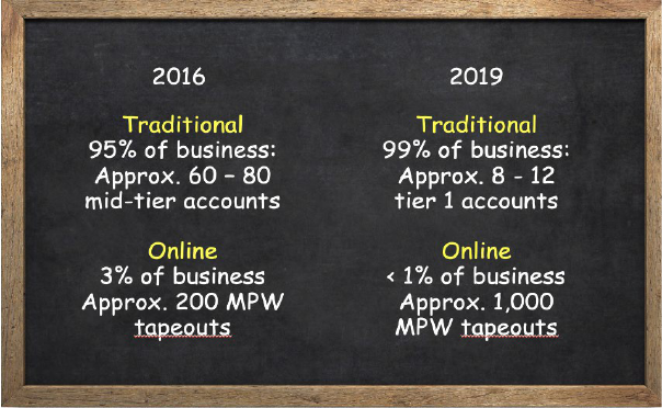
53
We added much more automation technology to our STAR platform as
well. The business, while small, was doubling year on year, with the promise
to grow even faster, as online businesses tend to do. In January, 2017, we
decided to shut down our online MPW business. The reasons for such a
radical decision require turning the page to the next chapter of eSilicon and
the ASIC business.
While our online business began around 2013, another trend began to
take shape around that time. The trend of consolidation in the
semiconductor industry. It began slowly at first but picked up steam along
the way. LSI Logic was bought by Avago. Then Emulex and few more.
And then Broadcom. What was once a focused, flexible top-end ASIC
company was now part of a massive, worldwide standard product
enterprise. During this same time, the mighty IBM Microelectronics, one
of the major players in the top-end of the ASIC market along with LSI
Logic, became part of GLOBALFOUNDRIES. There was more
consolidation during this time across the world.
The result of this macro trend was the creation of a “hole” in the top end
of the ASIC market. The companies that previously addressed this segment
were now part of larger enterprises. ASIC was a part of the equation, but
not the complete picture anymore. And these larger enterprises tended to
54
compete with their ASIC customers due to their large standard product
footprint.
Pure-play ASIC companies to address the needs of the top-end of the
market were needed. And eSilicon had the right profile to address these
needs. So, in January, 2017 eSilicon’s management team assembled for a
strategic planning session. Many options to blend our various businesses
were weighed, but one simple analysis, drawn on the whiteboard by our
CFO, drove the point home.
Our online business was a good one, but it didn’t fit with the dynamics
of our new opportunity to serve the top-end of the ASIC market—a
substantial and lucrative opportunity. So, we shut down our online
business. Between January and May of 2017, we did a record number of
MPW tape-outs and then we moved on.
The next chapter in eSilicon’s history has been quite exciting. It began
with one design win in the top-end of the ASIC market and then another
and more after that. Today, eSilicon focuses most of its energy serving this
market for the high-performance networking, computing, 5G
infrastructure, and AI segments. We’ve developed a substantial array of
differentiating semiconductor IP to address the unique needs of these
markets. While this shift is significant for eSilicon, there is a bigger shift
happening that is relevant for the entire ASIC market.
That shift has to do with what we’ll call ASIC success. When the first
version of this book was published, ASIC success meant handing off a chip
to the end customer that passed the manufacturing test program. Given the
levels of complexity and integration delivered by those designs, this model
worked. Today, it’s different. At the top end of the market, it’s often not a
chip that’s delivered by the ASIC vendor. Instead, it’s a highly complex
system-in-a-package that typically contains a massive, FinFET-class chip
and multiple 3D memory stacks integrated on a silicon interposer.
Passing the manufacturing test program is just the beginning of bringing
up a design like this in the target system. There are chip/package/system
55
interactions, the need to debug potential interactions between
semiconductor IP from multiple sources and hardware/software/firmware
interactions. In this environment, delivering the required performance of
the chip in the system context is the new measure of success. The task
is daunting, but rewarding. Hitting the mark on a new router or 5G
infrastructure component is quite lucrative for all involved. Getting there
isn’t easy, but clearly worth it.
In this new paradigm of what ASIC success means, eSilicon finds itself
playing the role of coordinator for multiple supply chain partners. The goal
of delivering the required ASIC performance in the system context does
take a lot of companies and a lot of coordination. It’s common in this new
world to have ALL departments involved in a design kick-off meeting.
System, chip, package, test, firmware and quality all have a role to play, and
all have to work in a coordinated fashion from the very beginning to stay
ahead of the curve. It’s also typical to assemble the bring-up team at the
customer months before the chip is out of fab to plan all the
hardware/software/firmware/package interactions required to achieve
ASIC success.
The systems that these new ASICs power will, undoubtedly, change the
world. eSilicon is proud to be part of the revolution.
57
Chapter 3: The FPGA
In the 1970s, a new type of electronic component emerged—the
programmable logic device (PLD). Electronic systems until that time were
generally built up out of integrated circuits called transistor-transistor logic
(TTL) devices that were made by semiconductor companies like Motorola,
Texas Instruments, and IBM. The TTL integrated circuits were small chips,
with a handful of basic logic operations and 16-20 pins connecting it to the
outside world. To make a system, like a computer or a calculator, you would
attach dozens or hundreds of these small integrated circuits onto a board,
perhaps along with some memory chips and a small microprocessor or
microcontroller.
These early TTL logic chips were made with bipolar junction transistors,
but were gradually replaced by a new technology based on metal-oxide
construction (MOS). This MOS technology developed into CMOS
technology (complementary metal-oxide semiconductor). CMOS, with its
improved performance and lower power use, allowed for the development
of the ICs we are familiar with today. CMOS became the standard
technology for ASICs, and made it possible to design larger
microprocessors and other large standard parts, such as display controllers
and UARTs (the serial interface of the day). Unlike TTLs, ASICs also
integrated all the ‘glue’ logic, the small bits of logic that tie the standard
components together.
CMOS-based ASICs were great for high volume products, like personal
computers, because the economics of semiconductors dictates that higher
58
volume means lower per-unit cost. You need to sell a lot of ASICs to cover
the high fixed costs of design and manufacturing. However, they are not as
good for applications that required small numbers of parts or where the IC
is extremely simple.
For these cases, semiconductor companies turned to programmable logic
devices (PLDs) which, unlike logic gates that have fixed functions, are
essentially blank slates that can be programmed to perform any number of
tasks. With PLD technology, a semiconductor company could realize the
economy of scale by manufacturing high volumes of ICs that the systems
company could then customize to fit any number of different products.
There were many variations on this technology, including programmable
array logic (PAL), field-programmable logic array (FPLA), generic array
logic (GAL), and the complex programmable logic device. In this chapter,
though, we focus on the FPGAs because they have been the most
successful and influential of the programmable devices.
PLDs Become FPGAs
The initial PLDs, which were brought to market in the early 1970s by
Motorola, Texas Instruments, General Electric, and National
Semiconductor, were very limited. One key limitation was the absence of flip-
flops, circuits that have two stable states and are used to store state
information. The early PLDs contained a small programmable memory that
could be used to configure the device. The memory was either a PROM
(programmable read-only memory), which could be programmed just once,
or an EPROM (erasable programmable read-only memory), which could
be programmed multiple times by erasing the old programming with
ultraviolet light (the package had a small quartz window for this purpose).
While PLDs continued to develop throughout the 1970s, another piece
of technology turned out to be even more important than the PLDs—gate-
arrays. Gate arrays, which we covered briefly in the ASIC chapter, is an
approach that uses wafers preprinted in volume with the transistors; only
the wires are added later to make it function as desired. Manufacturing the
59
gates, often called front-end-of-line or FEOL, was the slowest stage. Putting
the metal connectivity on, called back-end-of-line or BEOL, was quicker.
Programmable circuits took a leap forward when the company Xilinx,
founded in 1984, realized that they could combine the PLD and the gate-
array approach into what became known as field-programmable gate-arrays
(FPGAs). These chips contained uncommitted logic that was turned into
the required functionality by programming a memory. This allows the
device to be quickly programmed based on an application’s requirements,
and dramatically reduces time-to-market.
FPGAs used CMOS technology, which was an improvement over the
original bipolar transistor technology used for the original PLDs and
helped make FPGAs competitive with ASICs in low-volume applications.
While FPGAs were still slower, more expensive, and consumed more
power than ASICs, they didn’t have the high fixed costs and time-to-market
disadvantages of ASIC.
An important enabler for FPGAs was the design automation tools used
to program them, which gave the FPGA programmers the same experience
that ASIC designers had, initially based on schematic diagrams of the
desired functionality and later using register transfer languages such as
Verilog or VHDL. The complicated task of working out which memory
bits to set in the array in order to get the desired functionality was
completely automated.
As with PLDs, FPGAs were manufactured as identical parts in high
volume and it was the system manufacturer who would configure them.
Usually the memory (the PROM or EPROM) was actually a separate chip
and the data would be transferred from the memory into the FPGA itself
to configure it each time the system was first powered on.
How FPGAs Fueled the Fabless Business Model
The first company to focus solely on FPGAs was Xilinx, which is still
the market leader today. Xilinx was also a pioneer in the fabless
semiconductor business model. Instead of building a fab, as most
60
semiconductor companies had up to that point, Xilinx leveraged personal
relationships with the semiconductor division of Japan-based Seiko Epson.
The first Xilinx FPGA was created in 1985 in a mature 1.2 µm
manufacturing process. It ran at 18 MHz and had a 1000-gate equivalence,
meaning that it could be used to implement the functionality of about 1000
gates, even though it actually contained more like 20,000 gates.
Because Xilinx didn’t have its own fab, they had their FPGA
manufactured by other semiconductor companies. They had contracts with
a number of manufacturers to reduce the risk that they might lose supply
and also introduce competition into price negotiations. Then, in 1995, two
major pure-play foundries, UMC and TSMC, opened for business. Xilinx
moved all their new production to UMC, which was the start of a long
relationship between the two companies.
It turns out that FPGAs were not only good business for the foundries,
they were also important for helping the foundries ramp up new
manufacturing processes. Early in the process development, the foundry
needs designs with very high degrees of regularity; this lets them apply
statistical approaches to yield improvement. Memories once served that
role, but these days FPGAs are used. If an FPGA has 10,000 identical
structures on it, then it is relatively easy to find systematic failures in the
manufacturing process. Compare that with ASICs, which from a process
point of view are pretty random.
Xilinx and UMC pioneered the “virtual IDM” relationship, where the
fabless company has full access to the process technology and is an active
development partner. Xilinx and UMC worked together to develop the
process technology, create test chips, and so on. In fact, Xilinx had a whole
floor of one of UMC’s buildings for their own employees. FPGAs would
usually be the first volume parts in a new technology.
The long-standing relationship between Xilinx and UMC ended in 2010,
when Xilinx switched their allegiance to rival foundry TSMC for the 28 nm
process node. Rumors had the relationship ending as a result of 65 nm yield
61
problems and delays in 40 nm which allowed Xilinx’s main competitor,
Altera, to gain significant market share. As a result of moving production to
TSMC, Xilinx beat Altera to silicon on the 28 nm and 20 nm nodes which
encouraged Altera to move production to Intel at 14 nm.
Use of FPGAs
Early FPGAs were used largely as “glue” logic—the gates in a design that
are outside of the larger chips like microprocessors, memories and the like.
As FPGAs developed, they began to be used in designs that were subject
to frequent change, for example, in the networking world where standards
were changing rapidly. In these cases, you don’t want to wait until the
standards are finalized before starting the chip design. Alternatively, you
could implement the standard in software. However, because hardware still
offers higher performance than software (throughput in a router, for
example), FPGAs are a better choice.
For example, Cisco Systems, a company that designs and sells networking
equipment, typically uses FPGAs for all but its highest performance
routers. As FPGAs continued to develop, and got larger, they reached the
size that entire systems or sub-systems could fit on a single chip. This meant
that processors were needed on the FPGA. There are two ways this has been
done: by putting an ARM or PowerPC processor (or more than one) on the
FPGA as a hard macro, and by adding processors designed by the FPGA
companies (for example, Altera’s Nios processor) that are implemented
using the FPGA fabric itself.
Today, for low-volume systems, FPGAs are the implementation medium of
choice. Their big weakness, besides cost at high-volume, is that they
consume a lot of power. Consequently it is not possible to use them for
many mobile devices because it would make the battery life unacceptably
short. But for ‘tethered’ systems, the flexibility and low up-front cost are
very attractive.
Another use for high-end FPGAs, which are too expensive to go into
any sort of consumer product, is prototyping for systems-on-chip. FPGAs
62
are used extensively in emulation and hardware-accelerated simulation
products, where the hardware needs to change to match the target design.
They are well-suited to this application because verification of an SoC using
only software simulation has become too time-consuming. Creating an
early prototype version of the system in an FPGA, and then using that for
verification, is considerably faster. While an FPGA is much slower than the
actual silicon will be, it is much faster than software. Consequently, it is
possible to run software loads and boot operating systems on an FPGA.
As more and more systems involve complex hardware interacting with
complex software, the FPGA prototyping route will only become more
attractive.
FPGAs Need Design Automation and IP
Unlike with ASICs, where most of the electronic design automation
(EDA) tools are provided by the 3rd party EDA industry, the software
needed to design FPGAs has largely been provided by the FPGA suppliers
themselves. There are several reasons for this, not the least being that the
physical design tools are specific to the architecture of the fabric itself. Place
and route tools for FPGA are completely different at the basic code level
than those for ASICs.
There were some early attempts by EDA companies to make design
software for FPGAs, but as the market came to be dominated by Xilinx
and Altera, who provide their own tools, the economics of providing
FPGA design tools became unattractive. In addition, the price point at
which designers expected to purchase FPGA tools were an order of
magnitude lower than for IC design tools. Consequently the EDA industry
has largely ignored FPGAs.
A minor exception is seen in the existence of synthesis and floorplanning
tools for high-end FPGAs, made by companies like Mentor and Synplicity
(acquired by Synopsys in 2008). But the market has remained small because
high-end becomes mainstream over time, and the free tools from the FPGA
vendors become “good enough.”
63
FPGAs now also include silicon IP, just as in the non-FPGA world.
Increasingly, creating a large system-on-chip involves more assembly of
pre-designed blocks of IP than creating an original design. As systems rely
more on software, FPGAs take on the role of a specialized computer
consisting of a processor, peripherals, and perhaps some accelerators to act
as the “secret sauce.” The economics of providing IP for FPGAs has also
not been attractive until recently, so most of the IP, apart from some
processors, has been created by the FPGA vendors themselves.
In the early days of IP use in FPGAs, the IP blocks were relatively simple.
At that time, the great majority of design software and IP for FPGAs were
provided by the FPGA vendors directly. FPGA design tools are still largely
provided by the FPGA vendors and there is little economic incentive for
3rd parties to provide these design tools.
However, for IP targeting FPGAs it has become another story entirely.
As the size of FPGAs has grown, the complexity of the IP that can be used
in them has also grown—from MSI devices to large subsystem blocks such
as Ethernet MACs and controllers, PCIe interface blocks, SDRAM and
NAND Flash memory controllers, video and network-packet processors,
motor controllers, and even entire microprocessors.
The two major FPGA vendors directly supply microprocessor IP tailored
specifically to their FPGA hardware architectures, but they increasingly rely
on 3rd parties for specialized IP for applications such as networking, video
and image processing, graphics, motor control, and other complex
functions. This FPGA-specific 3rd-party IP runs through the FPGA design
tools’ design and logic-synthesis flow just as it does when designing chips
using ASIC and SoC EDA tools. As a result, there’s now a growing industry
for 3rd-party companies developing FPGA-specific IP.
The Future of FPGA
Innovation continues in FPGAs. Starting in 2011, Xilinx started using
through-silicon vias (TSVs) to build 3-dimensional chips. These are actually
called 2.5D because multiple individual die are stacked on a silicon
64
substrate called an interposer. True 3D has all the die stacked directly on
top of each other in a single package. A TSV is just what it sounds like, a
metal plug (usually copper) that runs from the top of the chip through the
entire wafer to the bottom where it attaches to the interposer. Xilinx
actually had the first 2.5D design in volume production.
In 2012, FPGA was about a $4.5 billion business. Xilinx has about 50%
market share at $2.2 billion. Altera is not far behind at $1.8 billion. Actel, now
part of Microsemi, and Lattice ($0.3 billion) are also significant suppliers.
Over the years, many startups have attempted to create FPGA
companies to compete with Xilinx and Altera. One barrier to the
entrepreneurs is that they run into patent infringement. Xilinx alone has
about 2,500 patents on FPGAs and related topics. Another challenge is
getting access to the leading-edge process technology that you need to be
competitive. Xilinx and Altera, in particular, have deep relationships with the
foundries and are likely to be ahead of any startup by a full process node.
However, two notable FPGA startups—Achronix and Tabula—have
potentially solved the “access to leading process technology” problem by
having Intel as an investor. Intel will manufacture their parts in 22 nm,
marking them as two of the first customers of Intel’s nascent foundry
business.
65
Update 2019: FPGA Landscape
In 2015 Intel acquired Altera for $16.7 billion, changing one of the most
heated rivalries (Xilinx vs. Altera) the fabless semiconductor ecosystem has
ever seen. Prior to the acquisition the FPGA market was fairly evenly split
between Xilinx and Altera with Lattice and Actel playing to market niches
in the shadows. There were also two FPGA startups Achronix and Tabula
waiting in the wings.
The trouble for Altera started when Xilinx moved to TSMC for
manufacturing at 28 nm. Prior to that Xilinx was closely partnered with
UMC and Altera with TSMC. UMC stumbled at 40 nm which gave Altera
a significant lead over Xilinx. Whoever made the decision at Xilinx to move
to TSMC should be crowned FPGA king. UMC again stumbled at 28 nm
and has yet to produce a production quality FinFET process so it really was
a lifesaving move for Xilinx.
In the FPGA business whoever is the first to a new process node has a
great advantage with the first design wins and the resulting market share
increase. At 28 nm Xilinx beat Altera by a small margin which was
significant since it was the first TSMC process node Xilinx designed to. At
20 nm Xilinx beat Altera by a significant margin which resulted in Altera
moving to Intel for 14 nm. Altera was again delayed so Xilinx took a strong
market lead with TSMC 16 nm. When the Intel/Altera 14 nm parts finally
came out they were very competitive on density, performance and price so
it appeared the big FPGA rivalry would continue. Unfortunately, Intel
stumbled at 10 nm allowing Xilinx to jump from TSMC 16 nm to TSMC 7
66
nm skipping 10 nm. To be fair, Intel 10 nm is closer in density to TSMC 7
nm than TSMC 10 nm. We will know for sure when the competing chips
are field tested across multiple applications.
A couple of interesting FPGA notes: After the Altera acquisition two of
the other FPGA players started gaining fame and fortune. In 2010
MicroSemi purchased Actel for $430 million. The initial integration was a
little bumpy but Actel is now the leading programmable product for
Microsemi. In 2017 Canyon Bridge (A Chinese backed private equity firm)
planned a $1.3 billion ($8.30 per share) acquisition of Lattice
Semiconductor which was blocked after US Defense officials raised
concerns. Lattice continues to thrive independently trading at a high of
more than $12 per share in 2019. Given the importance of programmable
chips, China will be forced to develop FPGA technology if they are not
allowed to acquire it.
Xilinx of course has continued to dominate the FPGA market since the
Altera acquisition with the exception of the cloud where Intel/Altera is
focused. Xilinx stock was relatively stagnated before Intel acquired Altera
but is now trading at 3-4X more than the pre-acquisition price.
Of the two FPGA start-ups, both of which had Intel investments and
manufacturing agreements, Achronix was crowned the winner with more
than $100 million revenue in 2018. Achronix originally started at Intel 22
nm but has since moved to TSMC 16 nm and 7 nm which will better
position them against industry leader Xilinx. Tabula unfortunately did not
fare so well. After raising $215 million in venture capital starting in 2003
Tabula officially shut down in 2015. They also targeted Intel 22 nm and
according to LinkedIn several of the key Tabula employees now work for
Intel.
According to industry analysts, the FPGA market capitalization broke
$60 billion in 2017 and is expected to approach $120 billion by 2026
growing at a healthy 7% CAGR. The growth of this market is mainly driven
by the rising demand for what we now call Adaptive Compute Acceleration
67
Platforms which include: AI in the cloud, Internet of Things (IoT), mobile
devices, Automotive and Advanced Driver Assistance System (ADAS), and
wireless networks (5G). However, the challenges of FPGAs directly
competing with ASICs continues but at 7 nm FPGAs will have increased
speed and density plus lower power consumption so that may change.
Especially in the SoC prototyping and emulation markets which are split
between ASICs and FPGAs.
69
In Their Own Words: Xilinx
As the first company to design and sell FPGAs, and still the largest,
Xilinx has a storied history of innovation and all the trial and error
involved in creating a new product and a new market. In this chapter,
Steve Leibson, strategic
marketing director at Xilinx, describes the
company’s role in the development of the FPGA, both from a
technology and a business perspective.
While working at microprocessor pioneer Zilog in the early 1980s, an
engineer named Ross Freeman conceived of a new logic circuit that was
reprogrammable: a single piece of silicon that could meet the needs of all
of those ASIC customers. At that time, there were dozens, perhaps
hundreds, of ASIC companies building custom silicon for thousands of
customers. However, the design and fabrication of ASICs took months.
Freeman’s idea would permit the development and implementation of a
custom IC in less than a day and it coincidentally hastened the birth of the
fabless semiconductor industry. Freeman earned a BS degree in physics
from Michigan State University in 1969 and a master’s from the University
of Illinois in 1971. He worked in the Peace Corps and taught math in
Ghana for two years.
When he returned to the United States, Freeman joined Teletype
Corporation and designed a PMOS (p-type metal-oxide semiconductor)
chip. Back then, PMOS calculator chips were the profitable, high-volume
LSI chips to make and PMOS was the process technology of choice
because PMOS logic was the easiest type of MOS logic to manufacture.
Therefore, it was also the cheapest type of logic to make. Freeman then
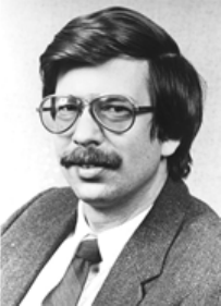
70
became one of the first engineers to join a new microprocessor startup
named Zilog where he designed the Zilog Z80-SIO (Serial I/O) peripheral
chip.
Ross Freeman, inventor of the FPGA.
By the time he reached his early 30s, Freeman was the Director of
Engineering for Zilog’s Components Division. He first got the idea for a
new type of hardware-programmable device while working at Zilog and
filed several patents. However, Zilog was not interested in pursuing the
concept so Freeman left Zilog to further develop his idea. The result came
to be known as the FPGA.
Although he had yet to develop a hardware design for this new device,
the invention was impressive enough for Freeman to sway a Zilog
coworker, Jim Barnett, to join him. The two of them then set out to recruit
their former boss at Zilog, an experienced executive named Bernie
Vonderschmitt, to become the CEO of the new FPGA start-up.
Semiconductor Business Lessons at RCA
Prior to joining Zilog, Vonderschmitt had worked for more than three
decades at RCA Corp. He was hand-picked by RCA’s legendary leader,
David Sarnoff, to head the color television development in 1953. Even
though the FCC had already approved it, Sarnoff was determined to
obsolete the rival CBS color TV system that was based on a mechanical,
rotating color wheel before it could spread commercially.
71
In an aggressive project over an 18-month period, Vonderschmitt’s team
at RCA developed the NTSC transmission standard. Unlike the CBS
version, it was backward-compatible with the existing standard for black-
and-white broadcast TV signals. Although often referred to by TV
engineers as “Never The Same Color,” the resulting NTSC broadcast
standard remained in use for half a century until it was finally replaced in
the United States by digital HDTV and the ATSC broadcast standard in
2009.
Partly because of his success in managing the NTSC color TV project,
Vonderschmitt eventually became the Vice President and General Manager
of RCA’s Solid State Division. RCA had developed semiconductors for its
own use in TVs, broadcast equipment and computers. The company waited
until the late 1950s before becoming a merchant semiconductor vendor.
Consequently, RCA missed the first IC manufacturing wave and did not
become a major player in the early bipolar integrated circuit market like
Fairchild. Instead, RCA focused on MOS integrated circuits. In the early to
middle 1960s, RCA’s David Sarnoff Research Center developed a way to
put both P- and N-channel transistors on one chip—demonstrating
feasibility in 1963 and 1964 and then developing the COSMOS (RCA’s trade
name for “complementary symmetry metal oxide semiconductor,” better
known as CMOS) line of integrated circuits in the late 1960s. Vonderschmitt
became head of RCA’s Solid State Division a bit later, in 1972. During that
period, Seiko came to RCA’s Solid State Division seeking to license a low-
power semiconductor process technology to help leapfrog its wristwatch
business. That’s when Vonderschmitt and Seiko first connected.
Seiko Epson Corporation had its origins in Suwa Seikosha, one of several
manufacturing companies in The Seiko Group. The Seiko Group evolved
from K. Hattori & Company, a trading company first established in 1881
that imported and exported clocks and watches. Suwa Seikosha was the
manufacturing arm of the company. It made men’s watches. Seiko had
foreseen the changeover from mechanical watches to all-electronic
wristwatches and it wished to be on the forefront of that change.
72
Vonderschmitt licensed RCA’s CMOS process to Seiko. By 1973, the
company was producing digital LCD wristwatches based on Seiko’s
proprietary CMOS watch chips.
While serving as head of RCA’s Solid State Division, Vonderschmitt had
a clear view of semiconductor manufacturing’s voracious appetite for capital;
he managed the company’s IC development and manufacturing businesses,
overseeing three in-house semiconductor foundries. During his tenure as
division head, Vonderschmitt often had trouble obtaining capital from the
parent corporation to scale new IC process technologies from the research
labs to production.
Things got more difficult as RCA moved further into its conglomerate
phase. David Sarnoff ’s son Robert Sarnoff had taken over the reins of the
company in 1970 and RCA announced its termination of the general-
purpose computer systems division in 1971, marking the company’s initial
move away from technology and the start of its conglomerate phase.
Making ICs was never RCA’s mainstream business. Producing televisions,
broadcast equipment, TV shows, and audio recordings on vinyl LPs were
RCA’s main businesses. During this period, RCA acquired Hertz (rental
cars), Banquet (frozen foods), Coronet (carpeting), Random House
(publishing) and Gibson (greeting cards). Consequently, those businesses
and RCA’s M&A activities garnered the lion’s share of the company’s
development capital leaving little for IC manufacturing growth and
development.
“If I Ever Start a Semiconductor Company, it Will Be
Fabless”
By the end of his tenure at RCA, Vonderschmitt was convinced that
captive semiconductor fabs were too expensive and too burdensome. “If I
ever start a semiconductor company, it will be fabless,” he vowed. “We’ll
find partners who can do our manufacturing for us.” With these insights
and his deep industry connections, Vonderschmitt had the vision and star

73
power that Freeman and Barnett would need to secure investors for a
fabless semiconductor company in 1984.
Vonderschmitt left RCA in 1979 and decided to take time off from the
industry. He used that time off to earn an MBA from Rider University.
Then he joined microprocessor pioneer Zilog in Silicon Valley. However,
Vonderschmitt joined Zilog after its startup days, just after it was acquired
by Exxon, and he soon saw that Zilog had the same problems with getting
capital for its fab and for improving its semiconductor process technology
from Exxon that RCA’s Solid State Division had with its parent. It was
“déjà vu all over again,” to quote Yogi Berra, and Vonderschmitt was ready
for a move when Freeman and Barnett approached him. Vonderschmitt,
Freeman, and Barnett officially founded Xilinx in February 1984.
Bernie Vonderschmitt, the originator of the fabless
semiconductor business model.
The Birth of Xilinx and the Fabless Movement
Although Freeman and Barnett convinced Vonderschmitt to found a
new semiconductor company based on the FPGA’s potential, he had no
intention of owning fabs as did RCA or Zilog. Having twice experienced
the stresses and risks of owning an IC fab, Vonderschmitt planned to focus
Xilinx on what Xilinx did best—designing innovative programmable
devices—and to partner with others to gain access to skills and assets not
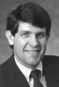
74
within Xilinx’s area of expertise, especially capital-intensive chip
manufacturing.
In pursuit of his vision for a fabless semiconductor company,
Vonderschmitt now leveraged his decade-long friendship with a Seiko
executive named Saburo Kusama to see if Seiko would be willing to
manufacture FPGAs for Xilinx. Vonderschmitt had met Kusama-san while
licensing RCA CMOS technology to Seiko for its watch business. In
pitching the Xilinx proposal, Vonderschmitt convincingly argued that such
a partnership would let Seiko keep its fab running at capacity to further
offset its capital equipment costs and possibly even make additional profit
if the Xilinx FPGA succeeded in the market. Vonderschmitt sweetened the
deal by granting Seiko exclusive reselling rights to Xilinx FPGAs in Japan.
The deal was consummated largely on the basis of the friendship between
Vonderschmitt and Kusama-san. The initial paper agreement was only two
pages long. Xilinx’s fabless business was launched.
The task of actually designing the first functional FPGA fell to a young
engineer named Bill Carter, whom Freeman and Barnett recruited from
Zilog in March 1984. Freeman had originally hired Carter at Zilog to work
on the Z8000 microprocessor. Carter now followed Freeman to Xilinx.
Prior to joining Xilinx, Carter had worked on NMOS microprocessors and
peripherals at Zilog and also had previous bipolar design experience. But
75
Seiko’s process technology was CMOS, so the Xilinx FPGA would be
Carter’s first CMOS design. As an added challenge, this FPGA was going
to be a very large chip. Thus Carter had to figure out a way to develop a
never-designed-before IC, which would be as large as a complex
microprocessor, on a very tight schedule. He also had to work with an IC
fab on the opposite side of the Pacific that was not accustomed to working
with outside customers all while overcoming barriers of a foreign language,
foreign business culture, and a foreign engineering culture.
Nothing Too Clever or Exotic
Vonderschmitt regularly advised Carter to keep the design as simple as
possible and not try anything “too clever or exotic.” An overly complex
design could make it harder to produce a functional device and deliver it to
customers on schedule. Keeping risk to a minimum was very important to
Vonderschmitt. He realized that a tiny start-up company offering a first-of-
its-kind chip through a unique fabless business model could easily scare off
customers.
In fact, to downplay the risk of doing business with the new FPGA
company, Vonderschmitt told would-be customers that Xilinx planned to
build a fab once it hit a US $50 million run rate and would also secure a
second source, as was customary—actually almost mandatory—at the time.
Monolithic Memories (MMI) later signed on as Xilinx’s first second source.
By coincidence, MMI was subsequently acquired by AMD, run by Jerry
“real men have fabs” Sanders, and so AMD became a second source for
Xilinx FPGAs. Seiko’s CMOS fab employed a 2.5 μm process—a relatively
mature and low-risk silicon process well suited to digital watch circuits.
Consequently, Seiko imposed very conservative design rules to make chip
manufacturing easier and to boost yields. The Xilinx FPGA design would
not be conservative with respect to design spacing. In fact, the XC2064
FPGA would require a whopping 85,000 transistors for its 64 configurable
logic blocks and 58 input/output (I/O) blocks. That was more transistors
than used in the design of the Motorola 68000 32-bit microprocessor. At
76
roughly 300 millimeters (mm) per side, the die size for the first Xilinx
FPGA would be larger than almost anything being manufactured at that
time and it would be much bigger than anything Seiko’s own designers had
ever attempted.
To keep the FPGA within the 300-mm spec, Carter knew he would have
to pack everything as close together as possible. He pushed Seiko to
thoroughly characterize its CMOS process and to provide extremely
accurate minimum feature sizes.
The chip’s architecture was largely based on one modular CLB
(configurable logic block) and one modular I/O block. The chip’s design
repeated these two blocks many, many times. (Some of the edge and corner
CLBs required slight variations.) The repetitive use of identical modular
blocks greatly simplified the FPGA’s design—enough to permit manual
design and verification. Xilinx used no computer-aided design (CAD).
CAD systems were too expensive for a semiconductor start-up on a
shoestring budget.
Carter’s design team employed extensive design reuse so that it could
concentrate the bulk of its time on circuit-level design and verification.
Despite Vonderschmitt’s urging to keep things simple, some of the chip-
design techniques that Carter used were unconventional. For example, a
typical CMOS design always pairs one p-channel transistor with an n-
channel device. Carter’s FPGA design drew on his NMOS design
experience and employed fewer p-channel and more n-channel devices,
which improved performance and saved space on the chip. The design
budget did allow Carter’s design team to lease SPICE simulation time on a
Control Data Corporation (CDC) mainframe, accessed via a dial-up
connection in those pre-Internet days. Remote SPICE simulation was
extremely slow. A simple syntactic error or typo could mean many lost
hours and waiting in the timeshare queue for the SPICE job to run only to
have that run fail because of a silly mistake was extremely frustrating,
particularly with a looming delivery deadline.
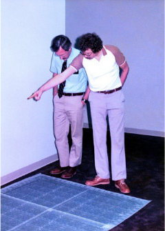
77
Ross Freeman checks a photoplot for the world’s first
FPGA, the XC2064.
Luckily, an inexpensive PC-based SPICE simulator became available at
just the right time. Carter convinced Vonderschmitt to invest in a PC,
which he used to verify that the SPICE deck syntax was correct before
submitting the simulation to the CDC mainframe. Although the PC ran the
SPICE simulation very slowly compared to the timeshare mainframe, the
elapsed time was about the same due to the additional overhead from the
upload speed over a modem and the waiting time in the timeshare queue.
The CDC time-share subscription quickly went away.
The team performed all design-rule checks, including electronic CAD
(ECAD) electrical rule checks to find simple errors, at the end of the design
process and then manually typed the final layout’s cell coordinates into a
Calma digitizer, which allowed the team to finally see the complete design
layout for the first time. After further checks, the team sent the nine-layer
design out to a pattern generator in preparation for mask production, which
was done by Seiko. The chip taped out in late May 1985.
The First FPGA Wafers Were Mostly DOA
After delivering the design to Seiko, Carter’s team had to wait two
months until early July, 1985 to receive the first-run silicon: a box of 25
78
wafers. The team applied probes, a home-brew debugger, and a curve tracer
to the wafers to see if any of the chips on the wafers would power up. The
first ten wafers out of the box all exhibited dead shorts between power and
ground. Not a good sign.
The 11th wafer showed some signs of life, and a very high current draw.
The last 14 wafers also had dead shorts between power and ground. Carter’s
team discovered that insufficient metal etching was causing the shorts.
There were aluminum whiskers causing shorts between the power and
ground rails all over the first-run wafers. On the single partly dead wafer,
the metal whiskers were thin enough to blow out like fuses. By applying
enough supply current to a chip on the wafer, the test team managed to
burn out the whiskers and open the shorts.
The Birth of the FPGA
Seiko and Xilinx solved the aluminum-whisker issue that plagued the
first-run batch of FPGA wafers and Xilinx received working devices in
September, 1985. A press release announced the birth of the world’s first
FPGA—the XC2064 (called a “Logic Cell Array” in the press release)—
on November 1, 1985.
The now-operational chips on that one wafer were sufficiently robust to
let Carter’s team continue debugging the design of the FPGA. Carter was
finally able to run a simple configuration bitstream into the device. After
successfully programming an inverter into one of the CLBs, Carter called
Freeman and Vonderschmitt while they were traveling in Japan and
reported that that the “DONE line had gone high,” and that Xilinx “had
successfully created the worlds most expensive inverter. After this initial
success, the design team was able to program more and different logic
circuits into the FPGA, eventually configuring all 64 CLBs on a chip.
In addition to providing an additional revenue stream to Seiko and helping
to keep the fab full, running FPGAs with their repetitive structures through
its fabs helped Seiko debug subsequent IC process technology generations,
improving device yields and lowering unit costs for all of the chips Seiko
79
manufactured. This use of FPGAs as a “process driver” helped to open the
door for Xilinx, giving the company access to leading-edge IC
manufacturing technology at Seiko and at other semiconductor foundries.
Fab vendors now want to use FPGAs as process drivers because of their
ability to diagnose process problems.
Conclusion
As the value proposition for the silicon foundry business became clear,
other IDMs started filling their fabs and supplementing their revenue by
manufacturing chips for third parties. In due course, an entirely new sub-
industry emerged of dedicated, merchant semiconductor foundries that
serviced fabless semiconductor vendors. This allowed even a small
company of entrepreneurial designers to realize their innovations in silicon
without the need to invest in a fab. The fabless revolution soon jumped
into high gear and in 1994, ten years after Xilinx was founded, several
fabless semiconductor companies including Xilinx formed the FSA (the
Fabless Semiconductor Association, now called the GSA or Global
Semiconductor Alliance) to provide a common voice to the electronics
industry.
Bernie Vonderschmitt had foreseen all of these changes back in the 1970s
while working for RCA. He knew from experience that fabs need more
than one corporate customer to keep the fab lines filled and the lights on.
He also understood that companies focused on IC design don’t need to and
often cannot afford to divert energy, resources, and attention to keeping
their fab processes at the leading edge.
As we’ve ridden Moore’s Law into nanometer territory through myriad
tectonic IC process changes (copper interconnect, immersion lithography,
high-K dielectric with metal gates, stress engineering, etc.), Vonderschmitt’s
fabless vision has become truer than ever. Over nearly thirty years, Xilinx
has worked with more than 20 different semiconductor vendors and has
partnered with ten vendors to supply its production FPGA silicon.
80
Vonderschmitt’s vision has sustained Xilinx through three decades of
FPGA leadership. The following words, written by Vonderschmitt two
decades ago and published in the Xilinx Xcell newsletter, are still as
accurate as the day they were written:
Making Fabless Strategies Work, by Bernie Vonderschmitt
(1993)
Xilinx is just one of the more than 100 semiconductor companies
that do not own their own fabrication facility, and use independent
silicon “foundries” for fabrication services. “Fabless” companies are not
a fad, their streamlined structure fits today’s tumultuous, fast-moving
marketplace. Being fabless allows Xilinx to concentrate on what we do
best—the design and marketing of programmable logic devices.
Hewlett-Packard’s announcement that it is quitting the foundry
business and the recent troubles of a few fabless companies have led
some industry pundits to once again question the viability of fabless
semiconductor suppliers. (Hewlett-Packard is not one of Xilinx’s wafer
sources.) We strongly believe that the oracles predicting the demise of the
fabless semiconductor are wrong. While ours is not the best business
model for everyone, Xilinx and many other fabless companies will
continue to succeed by establishing a win-win business relationship with
our foundry partners.
The first key to a successful fabless strategy is to employ standard
fabrication processes that are compatible with a variety of foundries.
Xilinx FPGAs and EPLDs are based on “plain vanilla” SRAM and
EPROM technologies. This allows us to benefit automatically from the
industry’s latest process improvements and to establish multiple foundry
sources for our products.
Multiple foundry sources ensure adequate and continuous product
availability in case of disasters. Competition between foundries, as well
as ongoing process and product
improvements ensure that price projections
are met. In contrast, fabless companies with specialized processes have
81
fewer potential suppliers and less leverage in the “foundry market.” If a
foundry agrees to a specialized process, prices inevitably will be higher due
to the special attention needed to get and keep that process under control.
The relationship between a fabless semiconductor company and its
foundries must be long term, based on mutual trust, and of benefit to
both parties. Xilinx benefits financially by gaining access to advanced
fabrication processes without huge capital investments. We can focus on
innovation, providing value through the development of better products.
Our foundry partners benefit from diversifying their manufacturing
capacity over different equipment markets; through Xilinx, they have
gained access to a significant new market segment without incurring the
expense of product and market development. Foundries minimize
demand volatility through this market diversification. Assuming a
long-term relationship, the foundry can improve its competitiveness
compared to other manufacturers.
Xilinx’s foundries have gained a significant additional benefit—the
ability to use FPGAs as process “drivers”—the technology used to drive
and verify process advancements.
The regularity and 100% testability of
our FPGAs facilitates defect analysis and fault testing.
Our foundries have learned that by applying 10% to 20% of their
capacity to FPGAs, they gain excellent rewards from process control
diagnostics. The resulting improvements
to their processes can be applied
to their other CMOS product lines. (It should also be noted that
Xilinx employs its own process experts, who work closely with our
foundry partners in the development and implementation of process
technology improvements.)
Thus, Xilinx can effectively drive process improvements through our
working relationships with our foundry partners. But these relationships
must be based on mutual benefits. In the future, as in the past, this will
be a necessary ingredient for success.
83
In Their Own Words: Achronix
Achronix has taken a long, circuitous, and ultimately very successful path
to becoming a successful semiconductor device and IP company. This
chapter describes the company’s development path from the initial idea to
develop the world’s highest-performance FPGA using asynchronous logic
to the company’s current role as the only semiconductor company to offer
FPGAs as chips, chiplets, and as embedded FPGA IP cores.
While most FPGA companies took root and grew up in Silicon Valley,
Achronix did not. Instead, Achronix was founded in Ithaca, New York by
John Lofton Holt, a successful business consultant who had worked at
PricewaterhouseCoopers and Booz Allen Hamilton and then later founded
his own technology consulting firm. He also became an entrepreneur.
Other founders included Dr. Rajit Manohar, a professor of electrical and
computer engineering (ECE) at Cornell University who has specialized in
asynchronous logic design for more than two decades; Dr. Clinton Kelly,
IV, who was one of Dr. Manohar’s PhD students and served as Achronix’s
first VP of Advanced Technology while managing most of the company’s
hardware engineering team for more than a decade; and Dr. Virantha
Ekanayake, who received his PhD at Cornell and then became an Assistant
Professor in the ECE Department at Johns Hopkins University where he
headed the Asynchronous VLSI and Architecture group before joining
Achronix full-time in 2006 as its CTO. These four people constituted
Achronix’s entire team for the company’s first two years.
84
Phase Zero: Brainstorming the Company
Holt met Manohar while searching for semiconductor technologies that
looked ripe for investment. At the time, very few investors were making
hardware/semiconductor investments and Holt believed that there was a
gap in the market that could be exploited with the right set of hardware
technologies. Manohar was pioneering asynchronous logic circuits at the
time. The two became friends. Manohar told Holt about a new, high-
performance asynchronous logic chip that his Cornell team had just taped
out. Holt and Manohar discussed the business possibilities for fast
asynchronous circuits on Holt’s front porch in Ithaca on a hot day in July,
2004. They discussed the benefits of asynchronous logic and technology’s
challenges. Holt then spent the next month determining where the
technology might be applied to best effect and for the biggest return on
investment.
High-end FPGAs had the best margins in the semiconductor business,
so Holt decided to attack the FPGA market with Manohar’s asynchronous
logic technology. The duopoly at the top of the FPGA pyramid, Altera and
Xilinx, were essentially offering identical FPGA products with very similar
performance characteristics and Holt’s research suggested that there was a
large and untapped market for FPGAs with significantly more performance
than the devices offered by the FPGA leaders.
Because of the FPGA’s compelling margins, more than a dozen startup
companies had jumped into the FPGA arena along with the four long-
established players: the Altera/Xilinx duopoly plus Actel and Lattice.
Nearly all of these FPGA startup companies had failed after collectively
burning through nearly a billion dollars in startup capital. All of these failed
startups offered some combination of unfamiliar silicon and unfamiliar
tools, so it was very difficult for them to find customers who would take
them seriously against the established players.
85
Despite the fact that all of these FPGA startups had failed, Holt felt that
Manohar’s asynchronous logic technology would give Achronix a clear,
competitive advantage over the more established FPGA vendors at
the high-performance end of the product spectrum. Holt’s research
suggested that there was a significant market for FPGAs that could deliver
more performance than even the high-end FPGAs available from the
Altera/Xilinx duopoly. Many prospective FPGA customers seemed willing
to pay a premium for that additional performance. But, having “familiar
silicon and familiar tools” was going to be essential to be successful.
Phase 1: Creating the Company
Based on Holt’s business analyses, the founders incorporated the
company on August 4th, 2004, and immediately set out to build an FPGA
that could deliver extremely high performance by leveraging the additional
speed made possible by using asynchronous logic. (All other FPGAs were
and still are based on synchronous logic.) However, offering devices based
on unfamiliar asynchronous logic design methodologies to FPGA users
that only knew how to design with synchronous circuits presented a real
problem. Worse, the mainstream EDA tools used to develop FPGA-based
designs only understood synchronous circuits.
To circumvent these basic market problems, Achronix designed an
FPGA that used asynchronous circuits internally to achieve high speeds
and then wrapped the asynchronous FPGA core with synchronous circuits.
The company also developed specialized design tools to mask the
asynchronous nature of the inner FPGA core so that it was not directly
visible to FPGA users. Engineers would design systems with Achronix
FPGAs using the same, familiar RTL design flow and familiar design tools
from leading EDA companies including Mentor Graphics and Synplicity,
while reaping the performance benefits of the asynchronous logic in the
FPGA core.
86
Achronix spent the first two years taping out a prototype asynchronous
FPGA in 180 nm silicon that achieved 650 Megahertz operation, which was
significantly faster than any competing FPGA technology at the time, while
simultaneously developing specialized design tools to de-risk the FPGA’s
asynchronous logic core. The specialized design tools integrated
seamlessly with the leading logic-synthesis tool for FPGAs – Synplicity –
which is still the leading FPGA synthesis tool today.
After proving the concept with the 180 nm FPGA device, Achronix
taped out a second FPGA in 90 nm technology. Holt recalls that he was
shopping in a grocery store in late 2005 when he got a call from Dr. Kelly,
who reported that the 90 nm silicon was back from the fab and was running
at 1.93 Gigahertz. The target had been 1.5 Gigahertz. Holt remembers
scaring most of the people in the grocery store when he let out a huge howl
of sheer delight at the news.
Achronix announced this achievement to the world in a press release on
April 24, 2006. Even today, in 2019, no commercial FPGA delivers
anything close to this performance. For the first time, a startup FPGA
company had developed a new and compelling FPGA technology with
familiar silicon and familiar tools.
At this point, Achronix had proven asynchronous FPGA technology by
delivering 4x to 5x more performance than competing synchronous
FPGAs available at the time. Holt packed his bags, left Ithaca, and spent
the next year trying to raise venture capital in Silicon Valley. It proved
extremely difficult. Two dynamics were in play. One was that VCs (venture
capitalists) just were not interested in investing money in chip startups at
the time. Worse, it seems that every big VC in the space already had at least
one failed or failing FPGA company in their portfolio. These VCs were not
looking to add another FPGA startup to their portfolios.
One other factor hampered the raising of venture money: Achronix’s
founding team did not fit the standard mold for a Silicon Valley chip
startup. The founders were not the typical bunch of Stanford grads who
87
had worked at Nvidia for ten years. They were a group of guys out of
Princeton and Cornell University on the East coast.
VCs fully understood the FPGA space. It was a high-margin, high-profit
semiconductor business and it was a very interesting space. However,
Silicon Valley VCs did not believe that any team, especially not one from
the East coast, could deliver. West coast VCs believed that semiconductors
were not really a thing back East, so they did not think that a founding team
from the East coast could successfully create an FPGA based on
asynchronous logic that would outperform FPGAs from the established
vendors. Further, they did not think that is was possible to make an
asynchronous FPGA look like the familiar, synchronous FPGAs or that an
asynchronous FPGA design flow could be fully compatible with the
familiar design flows based on the leading EDA tools.
In addition, Holt was all of 29 years old at the time; he simply did not fit
the standard mold for a startup semiconductor company’s CEO. For all of
these reasons, Holt found it very hard to convince the Silicon Valley VCs
to invest in Achronix, so he packed his bags once more, went back East,
and quickly landed VCs who were willing to take a chance on an FPGA
company based in New York state, partly because they did not yet have
failing FPGA companies in their portfolios.
Achronix moved from Ithaca to Silicon Valley in 2006. Holt packed his
car with one bag and a computer and arrived in San Jose thirty-nine hours
later after an overnight stay in Lincoln, Nebraska. Holt had built many
relationships in Silicon Valley and the coast-to-coast move allowed him to
attract high-quality talent from other semiconductor and FPGA vendors
including Actel, Altera, Lattice, LSI Logic, and Xilinx. (Very few people
living in the California climate are willing to move back East, where there
is snow and ice for big portions of the year.)
Because Achronix had not yet established a Silicon Valley headquarters,
the company met in a rented conference room at Marriott’s Fairfield Inn
& Suites on First Street near Norman Y. Mineta San Jose International
88
Airport for the first two weeks. During these early meetings, Holt absorbed
hard-earned knowledge about running an FPGA and semiconductor
company and about the FPGA market from his new recruits.
It is one thing to make an FPGA; It is quite another to sell them at a
profit on the open market against established competitors. In effect, Holt
was preparing for battle against larger, more established competitors.
However, he was buoyed by the fact that his new employees had left big
salaries and substantial financial packages to join his new FPGA startup.
He had recruited a team of believers.
Phase Two: Growing the Company
Over the next two years, Achronix focused on getting its first commercial
FPGA to market. As a startup, Achronix had to do many things in parallel:
build the product, build the team, and develop critical partnerships with
EDA vendors including Mentor Graphics and Synplicity. Early on, Holt
realized that his fledgling FPGA startup could not afford to have the
software-engineering staff needed to develop a full suite of EDA tools for
the company’s FPGAs. So, from the start, Achronix relied on existing best-
in-class tools from leading EDA vendors, which it would adapt for its
FPGAs. Even so, Achronix needed to hire a lot of people. Holt compares
the effort to building a car, you are building the factory to manufacture all
of the parts for the car, while you are building the assembly line that
assembled the cars. Everything needed to happen in parallel.
Achronix also partnered very aggressively on the IP side. It developed
close relationships with companies that provided essential IP such as
Snowbush Microelectronics. Achronix funded Snowbush’s development
of a multi-standard, high-speed SerDes that operated at one to ten Gigabits
per second. The company also partnered with True Circuits for other IP
cores and worked with ASIC specialist eSilicon. Through these
partnerships, Achronix successfully brought its first 65 nm product to
market, introducing it as the Speedster FPGA on September 16, 2008. The
89
original Speedster FPGA ran at over 1.5 Gigahertz – significantly faster
than any other FPGA on the market, then or now. The design flow that
encapsulated the FPGA’s asynchronous core worked so well that engineers
could easily use their existing, familiar EDA tools to design with the
Achronix FPGAs. Early-access customers successfully pushed designs
through the Achronix design flow.
A Serious Miscalculation
However, over the next 12 to 18 months, Achronix discovered that it
had seriously underestimated how important power consumption was to
FPGA users. Hardware engineers must almost always trade off speed
versus power when selecting any electronic technology and a 1.5 Gigahertz
FPGA necessarily draws a lot of power.
As a car enthusiast, Holt makes the following analogy. Bugatti’s $3
million Chiron automobile has a 16-cylinder, W-16 engine that develops
1200 horsepower. The car has a top speed of 261 miles per hour (420
kilometers per hour) but it gets four miles to the gallon and drains the gas
tank in ten minutes at that speed. Not a lot of people need a street-legal car
like that.
Ultimately, Achronix’s asynchronous Speedster FPGA drove several
million dollars in revenue. However, it quickly became apparent that
Achronix’s initial FPGA offering would not be the product to make the
company profitable, which of course was the ultimate objective. Achronix
needed to pivot its product strategy.
The company had developed a great team and a phenomenal software
design flow. It had also developed a semiconductor sales channel and a
great team of nearly 100 people. It had successfully brought an FPGA and
development tool suite to market with that small team – something that
established FPGA vendors needed thousands of people to achieve.
However, Achronix had essentially misread the market by
overemphasizing raw speed over power consumption. The market wanted
90
speed, but not at any cost. Power consumption was still a significant part
of the tradeoff equation. Achronix’s development team tried many ways to
reduce the power consumption of the asynchronous FPGA technology,
but ultimately decided to discontinue the use of asynchronous-logic
technology.
The First Pivot: Partnering with Intel
In 2010, Achronix pivoted its strategy to focus on building a synchronous
FPGA that leveraged a small bit of the company’s existing asynchronous
technology in some internal blocks. The new, synchronous FPGA was still
optimized for the high-performance, high-margin, high-end part of the
FPGA market, which essentially meant that the key target applications were
telecom and networking. The new synchronous FPGA design incorporated
a significant amount of hardened IP to maximize performance, but the
other prong of the high-performance strategy, that part that would
differentiate Achronix from the other FPGA players, was to partner with
Intel.
Achronix was the first company to cut a deal with Intel for the
manufacture of high-performance ICs based on Intel’s 22 nm, FinFET
process. The press release announcing this deal appeared on November 1,
2010 and said:
“The Achronix Speedster®22i FPGA family will shatter existing
limitations of FPGAs, allowing cost-effective production of high-
performance devices over 2.5M LUTs in size, equivalent to an ASIC of
over 20 million gates.”
Partnering with Intel rocketed Achronix into a very high-profile
trajectory. With that deal, Achronix leapfrogged its two large FPGA
competitors, Altera and Xilinx, which were using a 28-nanometer, planar,
CMOS process technology that delivered substantially less performance.
Although Achronix had left asynchronous logic behind, the company had
91
found a way to maintain its performance leadership by leveraging Intel’s
leading-edge process technology.
Achronix spent the next two years developing the Speedster22i FPGA
family. It was a huge design challenge, partly because Intel was not
established as a chip foundry. It was not TSMC. Intel’s chip-design tools
and design rules were unique to Intel. Although Achronix got a lot of
attention and help from Intel as its first foundry customer for the advanced
22 nm, FinFET process, the Speedster22i FPGA took much longer to build
and a lot more money than expected. On February 20, 2013, Achronix
announced that it had begun shipping the Speedster22i HD1000 FPGA to
customers.
The Second Pivot: A New President and CEO
After the Intel partnership announcement, Holt realized that he had been
working exclusively on Achronix as CEO for more than six years. It had
been a huge investment of his time and of his own money because Holt
had invested a big chunk of his personal wealth on the startup. He realized
that he needed someone new and fresh to help the company grow faster
and to eventually take it public.
Holt had known FPGA industry veteran Robert Blake, another
consultant, for several years. He and Blake had become friends and they
had an excellent, professional working relationship as well. Eventually, Holt
suggested that Blake take over as Achronix’s President and CEO. Holt says
that this decision was very, very difficult for him, personally. He’d put his
heart and soul into the company for several years and found it very hard to
let go of the reins. But, from his time as a management consultant to CEOs,
Holt knew that it was the right decision.
Ultimately, Holt did not fully release all of the reins. Holt and Blake
enjoyed working together and developed a divide-and-conquer strategy.
Blake became President and CEO and Holt became Achronix’s Chairman.
The public announcement of the management change came on April 15,
92
2011. This was an emotional and bittersweet moment for Holt, but he
quickly saw that he had made an excellent decision in hiring Blake.
The Third Pivot: Embedded FPGAs and Chiplets
Focusing exclusively on high-performance, high-margin FPGAs limited
Achronix’s TAM (total available market). There is a significant market for
mid-range and low-end FPGAs and Achronix could not address those
markets with the high-performance Speedster22i FPGA. The available
margins in those market segments could not support high-end devices
made in Intel’s highest-speed process technology, yet these markets are still
attractive because of their significantly higher product volumes. Achronix
needed a different product strategy to make forays into these lower-tier
FPGA markets, which were served by other FPGA vendors.
The new strategy developed as a result of the path that Achronix had
taken to develop its first-and second-generation FPGAs. Achronix had
developed a chip-design flow that treated the FPGA core as a standalone
IP core to accommodate the company’s initial strategy of wrapping an
asynchronous FPGA core in synchronous peripheral circuitry to make it
compatible with existing EDA tools. This design approach—developing
the FPGA core as a standalone IP block—was unique in the FPGA
industry and it suggested a similar, IP-based product for the lower-tier
markets. The new product would be an embedded FPGA or “eFPGA”: an
encapsulated design for an FPGA core that could be dropped into any
company’s SOC design. Coincidentally, the SOC market was just becoming
ready for such a product.
Achronix had been investing in eFPGAs since 2010 but there was a
significant problem. An eFPGA core requires a significant amount of
silicon real estate compared to most other IP cores, although not nearly as
much silicon as a complete FPGA due to many integration efficiencies such
as the lack of peripheral I/O circuits capable of driving traces on a circuit
board. Achronix had developed an embedded FPGA core for the 28 nm
process node, but it was not economically attractive. The 28 nm core
93
needed too much real estate. Early press reaction to Holt’s announcement
about these early investments in the eFPGA was skeptical, dismissive, and
brutal.
However, at the 16 nm process node, eFPGAs needed much less silicon
and were suddenly an economically viable alternative to separately
packaged FPGAs. Consequently, Achronix became the first eFPGA IP
core supplier, announcing the availability of the first eFPGA cores on
October 4, 2012 and instantly created the eFPGA market. Over the next
several years, Achronix successfully deployed eFPGAs into some of the
largest FPGA customers in the world, allowing them to build their own
SOCs with Achronix eFPGA technology, rather than buy expensive and
power-hungry FPGA chips from other vendors.
Achronix also jumped on board the relatively recent chiplet trend. The
company’s Speedchip product, a high-speed FPGA in chiplet form, is
optimized for multi-chip SiP (System in Package) designs. The Speedchip
chiplet communicates with a host ASIC or SoC via industry standard, high-
speed interconnect such as USR (ultra-short reach) or PCIe XSR
(eXtremely short reach) SerDes technology.
Thanks to the introduction of the Speedster22i FPGAs, Speedcore
eFPGA IP cores, and Speedchip FPGA chiplets, Achronix crossed over
into profitability in Q1, 2017. On June 14, 2017, the company announced
a 700-percent increase in year over year revenues and further announced
that it expected to cross $100 million in revenue by the end of fiscal 2017,
which it did. On February 5, 2019, the EDN Network named Achronix’s
Speedcore Gen4 eFPGA IP to its Hot 100 product list for 2018.
At this point, Achronix is the only vendor in the world to offer FPGAs
as chips, chiplets, and as IP cores, all served by the same ACE design tool
suite.
95
Chapter 4: Moving to the Fabless
Model
Before the mid-1980s, all semiconductor companies were what we now
call Integrated Device Manufacturers or IDMs. They developed their own
semiconductor process, purchased and ran their own fabs, and then sold
the resulting product.
Fabs were never cheap, but back then a fab was affordable to even
relatively small semiconductor companies. Aside from the capital costs of
the manufacturing equipment, there are two other costs associated with
having a fab: developing the manufacturing process and maintaining the
volume required for cost-effective manufacturing. In the early 1980s,
developing the semiconductor process was also affordable, and the volume
required for cost-effective manufacturing was not too high, so “filling the
fab” wasn’t difficult.
Over the next couple of decades, all three expenses associated with
running a fab changed. The cost to build a modern fab is now in the $10
BILLION-dollar range. The process development cost for a modern
semiconductor process is so high that only Intel and TSMC go it alone
today. Everyone else is in a semiconductor company club of some sort
where many of the costs of development are shared. For example, IBM,
Samsung, and GLOBALFOUNDRIES together formed the Common
Platform to collaboratively develop process technologies and populate the
96
vast ecosystem of EDA, IP, libraries, packaging, and design services needed
to bring a new design into existence.
Given the cost of building a modern fab and developing new process
technology, the fab production line needs to be kept full. The volume
required for cost-effective manufacturing runs into tens of thousands of
wafer starts per week, a number so high that very few semiconductor
companies can fill their own fab even if they could afford to build it. So
today, IDMs are an endangered species and most semiconductor companies
use foundries such as TSMC for all or most of their manufacturing. The
fabless and fab-lite models are probably the single most important
development since the invention of the integrated circuit in terms of its
impact on the growth of the semiconductor industry.
Early Fabless Companies
This fabless trend started in 1984 with the first true fabless semiconductor
companies—Chips and Technologies and Xilinx. Gordon Campbell, the
co-founder and CEO of Chips and Technologies, is usually credited with
realizing that a smaller semiconductor company could thrive without its
own fab. Apparently, as Campbell and the other founders were raising
funding for Chips and Technologies, the business plan included building a
fab, although they never intended to do so. They believed no one would
fund something as outrageous as a semiconductor company with no fab.
They also suspected that the fabless idea was so appealing that once it was
revealed, every venture capitalist they talked to would also start funding
competitors because the investment required was so much lower than for
an IDM.
Xilinx, founded in 1984, was a key early fabless semiconductor company.
Xilinx was in a completely different business from Chips and Technologies,
who built graphics chips for PCs, and they were not competitors. But their
business model was basically the same; design a small number of products
and pay another semiconductor company to manufacture the wafers.
97
Without the large fixed investment of its own fab, the amount of
investment required to get to market was much lower.
Another important early fabless semiconductor company was
Qualcomm. Founded in 1985, it was involved in a number of different
businesses, such as satellite location tracking used by long-haul truckers. In
1990, they developed the CDMA wireless standard, which was deployed in
the US by Sprint and Verizon and grew their business very quickly.
When Chips and Technologies, Xilinx, and Qualcomm were founded,
there were no pure-play foundries, companies that focus only on the
manufacturing of other people’s chips. However, semiconductor
companies with their own fabs regularly manufactured wafers for other
companies to even out an irregular production schedule. Any given
semiconductor company might need more wafers than their fab could
handle in one quarter, and then have extra capacity the next quarter.
Because so much of the cost of a fab is depreciation on the equipment, idle
production lines cost almost as much as busy ones, in the same way that an
empty airline seat costs almost as much as filling the seat.
A big advantage of the fabless model was shedding the high fixed cost of
running a fab. In effect, the fixed costs of a fab were changed to variable
costs. Fabless companies paid a little more per wafer by using someone
else’s fab, but this was offset by the money saved by not having to build,
run, and fill their own fab.
It was into this burgeoning new fabless semiconductor industry that the
first pure-play foundry, TSMC, was launched in 1987. It was pure-play in
the sense that it only manufactured and sold wafers for other companies.
It did not design any of its own products. Across the road from TSMC was
United Microelectronics Corporation, or UMC, which was founded as a
traditional semiconductor company (and also provided foundry services) in
1980. UMC became a pure-play foundry in 1995, and has ranked second to
TSMC until recently. The next chapter focuses on the foundry business in
more depth.
98
In the early days, TSMC and UMC mostly manufactured wafers for
semiconductor companies who had fabs but not enough capacity. There
was very little business from fabless companies. In fact, all the designs from
fabless semiconductor companies together could not have filled a single
fab in 1995. The balance would gradually change in favor of fabless
semiconductor companies and was driven by two trends. First, the creation
of more and more fabless semiconductor companies, which all required
manufacturing capacity; second, the gradual decline in the economic
attractiveness to semiconductor companies to own their own fabs.
When the then-CEO of AMD, Jerry Sanders, said “Real men have fabs,”
he was suggesting that chip design and process technology had to be tightly
coupled. One could argue what impact this has on a business. AMD
abandoned its fabs in 2009, and their main competitor, Intel, did not. For
all the missteps AMD has made in the market, it’s not clear that any of them
are due to the decoupling of design and manufacturing that resulted when
they went fabless. The world semiconductor rankings from iSuppli show the
shift towards the fabless model. As recently as 2007, there were no fabless
semiconductor companies ranked in the top ten. In 2012, the latest year for
which figures are available, Qualcomm is number three and Broadcom, also
fabless, is number nine, and at number 12, is the now-fabless AMD.
Today there is actually very little difference between the traditional IDMs
and the fabless companies. Most semiconductor design houses outsource
at least some of their manufacturing to foundries such as TSMC or
GLOBALFOUNDRIES. State-of-the-art fabs are so expensive that even
semiconductor companies that keep some of their manufacturing in-house are
forced to use foundries for their most advanced manufacturing at 28 nm,
20 nm, and below. Only a few IDMs—such as Intel, IBM, and Samsung—
have state-of-the-art fabs, although they also outsource some
manufacturing to the foundries.
The history of pure-play foundries and their role in shaping today’s
fabless semiconductor industry is an interesting story in itself, and in fact,
99
after the following history of fabless company Chips and Technologies, is
the topic of the next chapter.
101
In Their Own Words: Chips and
Technologies
Chips and Technologies (C&T) is known as the first fabless
semiconductor company. One of the founders, Dado
Banatao, spoke to author Paul McLellan about starting the
company and launching the business model that would
eventually be dominant in the industry.
In 1985, Dado Banatao and Gordon Campbell started a company called
Chips and Technologies. Campbell, along with Bernie Vonderschmitt of
Xilinx, is credited with pioneering the new, fabless, business model.
Disruptive new concepts usually meet with resistance by the establishment,
and in fact Banatao, whom today is managing partner at Tallwood Venture
Capital, said that they had a hard time raising money because VCs couldn’t
comprehend a fabless semiconductor company. Even his friends told him
it “wasn’t a real semiconductor company.” In fact, the first $1 million was
raised from a real-estate investor! Only after they were further along were
they able to raise another $3 million from various Japanese investors,
including the large Japanese conglomerate, Mitsui Group.
They made a technical decision to use gate-array, rather than standard-
cell design, because the booming PC business created a sense of urgency in
getting their chipsets to market. They chose the industry-leading gate-array
technology from Toshiba, but then found that their design was too large
for even the biggest gate-array. The solution was to partition the design
into two chips: one logic CMOS gate-array from Toshiba and a separate
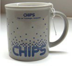
102
bipolar chip with all the IO drivers that Hitachi fabricated. Hitachi had a
lot of available fab capacity due to the semiconductor downturn at the time
and was somewhat desperate for business. C&T filled up those fab lines
completely, and got unbelievably low prices.
C&T’s business took off fast. C&T sold chipsets for IBM’s PC-XT and
PC-AT, and made $12 million profit in the first four months after their
chipset was introduced. By the time they had their IPO in 1987, just 22
months after opening, they still had $1 million of their original $4 million
investment in the bank. The fact that Mitsui was an investor turned out to
be fortuitous because Toshiba and Hitachi were part of the Mitsui Group.
This let them order parts from Toshiba and Hitachi without having to pay
up-front with working capital that they didn’t have. Mitsui financed $50
million in inventory.
C&T products dominated for about two years before their competitor,
VLSI Technologies, started selling their first chipset. C&T’s bipolar chip
turned out to have the advantage, since at that time electrostatic discharge
(ESD) protection on the CMOS technology favored by VLSI was in its
infancy and was still a potential problem. This let C&T make the claim of
better reliability compared to VLSI’s all-CMOS solution. Three years later
C&T’s chipset was all CMOS too, but by then ESD protection was up to
20 KV and those issues had gone away.
Banatao left C&T in 1989 to launch another start-up, S3 Graphics, which
focused on graphics processors. S3 Graphics also used the gate-array
technology to get to market fast. They looked around for the biggest arrays
and found what they needed at Seiko-Epson. Banatao’s key invention at S3
103
was a new interconnect, a local bus, to move between chips faster. They
called it Advanced Chip Interconnect, which later became Intel’s PCI and
PCIe.
C&T also sold chipsets to Dell very early on and they rode the PC rocket
together. While Compaq was the top PC maker at the time, they didn’t yet
believe in using chipsets. Before long, Taiwan, Korea, and Japan were all
making PCs. Compaq couldn’t compete, so they switched from single chips
to chipsets too. Interestingly, at that point in the industry history, C&T was
making more on each PC than Intel was.
Gordon Campbell, who had come from Intel and had a previous startup
called SEEQ Technology, left the C&T in 1993 to found 3Dfx Interactive
and has been involved with many other successful companies since then.
By the time he left C&T, the company had been suffering from lower sales
and big losses. The new president and chief executive officer, Jim Stafford,
managed to get them back to profitability by restructuring the management
and some product lines.
C&T went on to become one of the largest suppliers of graphics
processors for notebook PCs. They began to work with Intel and Lockheed
Martin on a new graphics chip for desktop PCs and workstations, the
Intel740, which was unveiled in early 1997. This collaboration proved to be
more than was evident at the time. By July 1997, Intel’s all-cash offer of
about $400 million to acquire C&T was a done deal. This was Intel’s largest
acquisition ever.
The impact of the new fabless business model started by C&T can’t be
understated. This is by far the dominant model for the semiconductor
industry today.
105
Chapter 5: The Rise of the
Foundry
The fundamental economics of the semiconductor industry is summed
up in the phrase “fill the fab.” Building a fab is a major investment. With a
lifetime of just a few years, the costs of owning a fab are dominated by
depreciation of the fixed capital assets (the building, the air and water
purification equipment, the manufacturing equipment, etc.). This puts a big
premium on filling the fab and running it as close to capacity as possible. If
a fab is not full, then the fixed costs will overwhelm the profit on the capacity
that is used and the fab will lose money. Of course, if demand is high there
is a corresponding problem because a fab that is already full cannot, by
definition, manufacture any more.
The capacity of a fab usually meets most of the overall needs of the
company that built it, but there can be a mismatch between the capacity
needed, in terms of wafer-starts, and what is available. Sometimes, the fab
is full, but the semiconductor company could sell more product if only they
could have manufactured it. Other times, the fab has surplus capacity, and
the semiconductor company doesn’t have enough product to keep the fab
full. This need to balance fab capacity and demand led to the original
foundry businesses, in which semiconductor companies, even competitors,
bought raw manufactured wafers from each other.
The first fabless semiconductor companies, such as Chips and
Technologies and Xilinx, extended this model a little bit. By definition, they
106
didn’t have their own fabs, but they would form strategic relationships with
semiconductor companies that had excess capacity. The relationships had to
be strategic: you couldn’t just walk into a semiconductor company and ask
for a price for a few thousand wafers, any more than today you can walk
into, say, Ford and ask how much to have a few thousand cars
manufactured. It is not how they are set up to do business.
Along Comes the Pure-Play Foundries
In 1987, a major change in the semiconductor industry took place with
the creation of TSMC. It was an outgrowth of Taiwan’s Industrial
Technology Research Institute, ITRI. Because very few fabless
semiconductor companies existed back then (Chips and Technologies was
founded only in 1985 for instance), the TSMC business model was to
provide manufacturing services to semiconductor companies who were
short of capacity in their own fabs. One of the original investors in TSMC
was Philips Electronics (since spun-out from Philips as NXP), who was
also one of the first customers buying wafers from them.
UMC, was an earlier spinoff from ITRI, created in 1980 as Taiwan’s first
semiconductor company. Across the road from TSMC in Hsinchu, its
focus also gradually shifted to foundry manufacturing, especially once the
fabless ecosystem created both a lot of demand and a wish to have a
competitor to TSMC to ensure that pricing remained competitive.
The third of the big three pure-play foundries back in that era was
Chartered Semiconductor. Chartered was based in Singapore and backed
by a consortium that included the Singapore government, who saw
semiconductor manufacturing as a strategic move up the electronic value
chain from contract manufacturing.
With the creation of TSMC, it became possible for semiconductor
companies to have wafers manufactured without requiring a deep strategic
relationship. Pricing wasn’t so transparent that you could just look at the
price-list on the web (plus, in 1987 there wasn’t a web) but a salesman would
quote you for whatever you needed. It was very similar to a metal foundry,
107
where the name had come from; if you wanted some metal parts forged, the
foundry would give you a quote and build them for you. In the same way,
if you needed some wafers manufactured you could simply go and get a
price.
This might not seem like that significant a change, but it meant that
forming a fabless semiconductor company no longer depended on the
founders of the company having a huge amount of capital to build a fab or
some sort of inside track with a semiconductor company with a fab. They
could focus on doing their design safe in the knowledge that when they
reached the manufacturing stage, they could simply buy wafers from
TSMC, UMC, or other companies that had entered the foundry business.
Companies such as TSMC and UMC were known as pure-play foundries
because they didn’t have any other significant lines of business.
Semiconductor companies with surplus capacity would still sell wafers and
run their own foundry businesses, but they were always regarded as a little
bit unreliable. Everyone suspected that if the semiconductor company’s
business expanded, then their fab would close to outsiders, forcing the
companies using that fab to find a new supplier. Gradually, over time, the
semiconductor companies whose primary business was making their own
chips became known as IDMs. This is in contrast to the fabless ecosystem,
in which the companies that create and sell the designs (the fabless
semiconductor companies), are separate from the companies that
manufacture them (the foundries).
Foundries Drive the Transformation from IDM to Fabless
The line between fabless semiconductor companies and IDMs has
blurred over the last decade. Back in the 1990s, most IDMs manufactured
most of their own product, perhaps using a foundry for a small percentage
of additional capacity when required. But their own manufacturing was
competitive, both in terms of the capacity of fab they could afford to build,
and in terms of process technology.
108
Gradually, both of these things changed. The size of fab required to
remain cost-competitive continued to increase to the point that most
semiconductor companies could not fill a fab that large. In 2002, the CEO
of Intel, Paul Otellini, estimated the cost of building a new fab at $2 billion.
Samsung spent $4 billion to build a fab in 2006. Estimates in 2013 for new
fabs in the planning stages for GLOBALFOUNDRIES and Intel hover
around $10 billion. The semiconductor processes also got significantly
more complex and costly, so that the cost of staying on the leading edge
became prohibitive for all except the largest IDMs, most notably Intel,
IBM, and Samsung.
The first key change away from the dominance of IDMs was the
formation of several process clubs, cooperative deals in which much of the
cost of semiconductor process technology development is shared between
a number of semiconductor companies. One early processor club was the
1992 alliance between IBM, Toshiba, and Siemens to develop memory chips.
A small semiconductor company couldn’t hope to develop a state-of-the-art
process on its own.
It quickly became clear that only the largest semiconductor companies
could afford to build a cost-competitive fab. It wasn’t just a matter of the
investment required, but also that there would be more capacity than they
would be able to use. Back when a fab cost $3 billion to build, a company
would face a depreciation cost of roughly $1 billion per year, meaning that
they need to have a running semiconductor business of perhaps $5 billion,
around the size of AMD, who was the only competitor to Intel in the x86
microprocessor business.
In fact, in March 2009, AMD, who’s CEO was famous for the “Real men
have fabs” comment, went completely fabless. They divested their
manufacturing to the Advanced Technology Investment Company,
primarily owned by the Emirate of Abu Dhabi. The manufacturing part
became the pure-play foundry GLOBALFOUNDRIES, although AMD
maintained a stake in the new foundry and was its largest customer.
109
Subsequently, GLOBALFOUNDRIES acquired Chartered
Semiconductor and today it is the second largest foundry behind TSMC.
Many other semiconductor companies also went fabless, such as
Freescale, Infineon, and Sony. Other semiconductor companies didn’t go
quite so far. They kept their existing fabs, many of which were fully
depreciated and running non-leading-edge processes. But for the most
advanced processes, they used the pure-play foundries because they
couldn’t afford either the investment or the cost of technology
development to keep up.
In the meantime, some IDMs also entered the foundry business. They
are not pure-play foundries since they also have a merchant semiconductor
business as well, but they are leveraging their leading-edge process
capability by selling wafers too. The three most significant of these IDMs
with a foundry business are Samsung, IBM, and Intel.
Samsung is Apple’s largest semiconductor supplier despite also being
their leading competitor in the smartphone market. It is also true the
other way around; Apple is Samsung’s largest foundry customer. In 2012,
Samsung overtook UMC to become the 3rd largest foundry.
IBM consumes most of their product internally to build computer
systems but also does a certain amount of foundry business, such as
building the logic chip for Micron’s hybrid memory cube.
Intel has also entered the foundry business. Initially, most of its
customers have been in the FPGA business, most notably Altera (the
second biggest FPGA company), which is using Intel’s 14 nm process. Intel
has also invested in, and is doing the manufacturing for, a few FPGA
startups such as Achronix and Tabula. However, Microsemi (which
purchased Actel, another FPGA company) also selected Intel as a foundry
and is using their 22 nm process. There have also been reports that Cisco
is using Intel as a foundry.
Today, the foundry model has split into two separate businesses. At the
leading edge, currently 22/20 nm and 14/16 nm, there are just a handful of
110
foundries with the financial and commercial muscle to build a state-of-the-
art fab. For pure-play foundries, there is TSMC and
GLOBALFOUNDRIES, and UMC with more limited capacity. TSMC has
fabs in Taiwan for these nodes, and GLOBALFOUNDRIES is running 28
nm in Dresden and building a brand new fab in Malta, New York. These
are the foundries that can build the latest smartphone SoCs such as those
by Apple, nVidia, and Qualcomm.
The other leading-edge foundries are the IDMs with a foundry business:
Intel, with fabs in Oregon, Arizona, and Ireland (and many more fabs in
other places), and Samsung, with fabs in Korea and Texas. IBM has its
leading edge fab in East Fishkill, New York.
The transition from IDMs to the foundry model has been quite dramatic.
At 130 nm there were 22 IDMs with their own fabs. By 45 nm this was
down to nine IDMs and five foundries. At 22 nm there is only Intel,
Samsung, and IBM as IDMs along with TSMC, GLOBALFOUNDRIES,
UMC, perhaps SMIC, and Samsung as foundries. At 14/16 nm the list
looks like it may shrink again. These companies are the only ones that have
announced fabs manufacturing at process nodes below 20 nm.
Every other semiconductor company is either fabless or fab-lite for these
leading-edge process nodes. The adoption of these advanced nodes is
driven by microprocessors (for Intel) and smartphones (for everyone else),
very high volume businesses that need the highest possible performance
and the lowest possible power.
The other part of the foundry business is not focused on the leading edge
but on designs for analog, power management, micromechanical, and so
on. For these designs, the state-of-the-art process today is 130 nm and so
does not require the most leading-edge fab. The Chartered fabs that
GLOBALFOUNDRIES acquired run this type of business, as do some
other specialized fabs such as Tower/Jazz and Vanguard, both of which are
pure-play foundries. There are also some IDMs running this sort of
business, such as PowerChip and MagnaChip.
111
Foundries Grow, Fabless Grows
Data from the GSA show that in 2013, the top foundry is TSMC by a
long way, with 2013 revenues of $20.1 billion. GLOBALFOUNDRIES is
number two with revenues of $5.1 billion. The third largest company in
terms of foundry business is Samsung (which is an IDM) at $4.6 billion,
followed by UMC with $3.965 billion. Fifth on the list is China-based
SMIC, the only other company with foundry revenues over $1 billion, at
$1.970 billion. The size of business drops off rapidly although there is a
long tail of foundries. For example, in twelfth place is Korea-based
MagnaChip with revenues of $440 million, less than one-fortieth the size
of TSMC.
A forecast from IC Insights published in the GSA 2014 IC Foundry
Almanac shows foundry revenues (both pure-play and IDMs) are expected
to increase 15% in 2014 to a record-high $51.1 billion. This follows a 14%
growth in 2013 and 21% growth in 2012. Foundries are now responsible
for more than one-third of IC sales worldwide. By 2017, foundry
manufactured ICs are expected to represent 45% of the industry’s total
integrated circuit revenues.
More and more of the top ten non-memory semiconductor
manufacturers are fabless and fab-lite companies. In iSuppli’s 2013
preliminary rankings Intel (IDM), Samsung (IDM and foundry), and
Qualcomm (fabless) take up the top three places. They are followed by
Micron (memory), SK Hynix (memory), Toshiba (fab-lite), Texas
Instruments (fab-lite), Broadcom (fabless), ST Microelectronics (fab-lite)
and Renesas (fab-lite). Basically, the rest of the top 20 are all either
completely fabless, take the fab-lite approach of using foundries for the
leading-edge process while internally manufacturing anything that doesn’t
require a leading-edge fab, or they are specialized analog suppliers who
don’t use leading-edge processes at all. IBM (IDM and foundry) slots in
somewhere, but they consume so much of their silicon internally that it is
not clear where. Their merchant business is not very large.
112
In the future, it is unclear whether all the IDMs and foundries that have
made the move to 22 nm will be able to afford to make the transition to
14/16 nm, and subsequently to 10 nm and 7 nm. There are big technical
challenges as well as economic issues as to what wafers will cost. As a result,
just how much of the existing product lines will make the transition to new
process nodes, as opposed to remaining on cheaper, less advanced, process
nodes is unclear.
An additional wrinkle is that it is not clear whether the cost per million
transistors—a key measure of the value of migrating to smaller process
nodes—will continue to decline as it has for the past 40 years. One view of
the world is that 28 nm might be the cheapest process by this metric. Of
course, at 20/22 nm and 14/16 nm there are gains in performance and
reductions in power, but the cost reduction that has always accompanied a
process transition may not materialize, or at the very least will be
significantly reduced. The old rule of thumb for a process transition was
that you get twice as many transistors at a 15% increase in wafer cost,
meaning a cost reduction of 35%. It remains to be seen how costs will
change going forward.
One technology that the industry has hoped would allow Moore’s Law to
continue is EUV lithography. It has been delayed for years, and while the
industry has invested heavily in the technology, it still cannot achieve high
enough wafer throughput to be used for high-volume manufacturing, and it
remains unclear if and when it will be. However, it also offers the
opportunity for a significant decrease in the time required to manufacture
wafers and a corresponding reduction in costs.
In the next two chapters, TSMC and GLOBALFOUNDRIES describe
their histories and roles in the development of the foundry business model.
113
2019 Update: Foundries
The semiconductor foundry landscape changed in 2018 when
GLOBALFOUNDRIES and Intel paused their leading-edge foundry
efforts. Intel quietly told partners they would no longer pursue the foundry
business and GF publicly shut down their 7 nm process development and
pivoted towards existing process nodes while trimming headcount and
repositioning assets.
Moving forward this puts TSMC in a much more decisive position in the
foundry landscape which has been talked about by the mainstream media.
The interesting thing to note is that the semiconductor foundry business
was based on the ability to multisource a single design amongst two, three
or even four different foundries to get better pricing and delivery. That all
changed of course with 28 nm which went into production in 2010.
TSMC chose a different 28 nm approach than Samsung,
GLOBALFOUNDRIES, UMC and SMIC which made the processes
incompatible. Fortunately for TSMC their 28 nm HKM gate-last approach
was the only one to yield properly which gave them a massive lead that had
not been seen before. While Samsung and GF struggled along with gate-
first HKM, UMC and SMIC changed their 28 nm to the TSMC gate-last
implementation and captured 2nd source business from TSMC following
the long-time foundry tradition.
Again, it changed back to single-source when FinFET technology came
to TSMC in 2015. FinFET is a complicated technology that cannot be
cloned without a licensing agreement. TSMC started with 16 nm followed
114
by 12 nm, 10 nm, 7 nm (EUV), 6 nm (EUV), and 5 nm (EUV) which will
arrive in 2020. Samsung licensed their 14 nm to GF which is the only
second sourced FinFET process. Samsung followed 14 nm with 10 nm, 8
nm, 7 nm EUV, 6 nm EUV, and 5 nm EUV. Pretty much a one-to-one
FinFET match-up between Samsung and TSMC. Today there are only two
leading-edge foundries left, TSMC and Samsung. TSMC is currently the
foundry market leader and I see that increasing when mature CMOS
process nodes that have second, third, and even fourth sources become
obsolete and the unclonable FinFET processes take over the mature nodes.
If you look at TSMC’s Q4 2018 revenue split, 50% is FinFET processes
and 50% is mature CMOS nodes (Q4 2018). In Q4 2017 FinFET processes
were 45% and in Q4 2016 it was 33%. As the FinFET processes grow so
does TSMC’s market share and that will continue for many years to come.
As it stands today TSMC has revenues of $34.2 billion in 2018. Revenue
growth in 2019 may be limited due to the global downturn but TSMC
should continue to claim market share due to their FinFET dominance.
In 2018 GLOBALFOUNDRIES, the #2 foundry, pivoted away from
leading edge process development (7 nm/5 nm) to focus on mature
processes (14 nm, 28 nm, 40 nm, 65 nm, 130 nm and 180 nm) and the
developing FD-SOI market with 22FDX and 12FDX following that.
In 2018 UMC, the #3 foundry, still struggled with 14 nm which forced
longtime ASIC partner Faraday to sign an agreement with Samsung
Foundry for advanced FinFET processes. Today, UMC relies on mature
process nodes: 28 nm, 40 nm, 55 nm, 65 nm, and 90 nm for the bulk of its
revenue from a select base of high-volume customers. Even when UMC
perfects FinFETs at 14 nm it will not be TSMC compatible so the market
will be limited. UMC’s 2018 revenue of $5.02 billion, being the second
largest publicly traded foundry (GF is private).
Samsung, the #4 foundry, is in production at 45 nm, 28 nm, 28FDSOI,
18FDSOI, 14 nm, 11 nm, 10 nm, 8 nm, 7 nm EUV, 6 m EUV and 5 nm
EUV. Samsung is a fierce competitor and gained significant customer

115
traction at 14 nm splitting the Apple iPhone business with TSMC. Even
today Samsung is a close second to TSMC in 14 nm if you include GF 14
nm which was licensed from Samsung. Samsung was also the first to "full"
EUV at 7 nm. Samsung's largest foundry customer of course is Samsung
itself being the #1 consumer electronics company. Qualcomm is also a very
large Samsung Foundry customer amongst other top fabless
semiconductor companies including IBM and AMD. The foundry business
was always about choices for wafer manufacturing so you can bet Samsung
will get their fair FinFET market share moving forward, absolutely.
In 2018 SMIC, the #5 foundry, also struggled with FinFETs. Mass 14
nm production is slated to begin in 2019, again it is not TSMC compatible
but in China it does not necessarily have to be. Today SMIC is
manufacturing 90 nm and 28 nm wafers mostly for fabless companies in
China. When 14 nm hits high volume manufacturing the China FinFET
market will likely turn to SMIC in favor of non-Chinese 14 nm fabs as it
did at 90 nm and 28 nm. The challenge SMIC has always faced is yield and
capacity and that will continue. In 2018 SMIC recorded sales of $3.36
billion with the majority of it based in China.
For a more detailed comparison of 7 nm and 5 nm see the analysis below
from Scott Jones of IC Knowledge dated 5/03/2019 www.semiwiki.com.
TSMC and Samsung 5 nm Comparison
Samsung and TSMC have both made recent disclosures about their 5 nm
process and I thought it would be a good time to look at what we know
about them and compare the two processes. A lot of what has been
announced about 5 nm is in comparison to 7 nm so we will first review 7
nm.
7 nm
Figure 1 compares Samsung’s 7LPP process to TSMC’s 7FF and 7FFP
processes. The rows in the table are:
116
1. Company name.
2. Process name.
3. M2P – metal 2 pitch, this is chosen because M2P is used to
determine cell height.
4. Tracks – the number of metal two pitches in the cell height.
5. Cell height – the M2P x Tracks.
6. CPP – contacted polysilicon pitch.
7. DDB/SDB – double diffusion break (DDB) or single diffusion
break (SDB). DDB requires an extra CPP in width at the edge
of a standard cell.
8. Transistor density – this uses the method popularized by Intel
that I have written about before in which two-input NAND cell
size and scanned flip-flop cell sizes are weighted to give a
transistors-per-millimeter metric.
9. Layers – this is the number of EUV layers over the total
number of layers for the process.

117
10. Relative cost – using Samsung’s 7LPP cost as the baseline we
compare the normalized cost of each process to 7PP. The cost
values were calculated using the IC Knowledge – Strategic
Cost Model – 2019 – revision 01 versions for a new 40,000
wafers per month wafer fabs in either South Korea for
Samsung or Taiwan for TSMC.
Figure 1. 7 nm comparison.
Looking at Figure 1 it is interesting to note that Samsung’s 7LPP process
is less dense than either of TSMC’s processes in spite if using EUV and
having the smallest M2P. TSMC more than makes up for Samsung’s tighter
pitch with a smaller track height and then for 7FFP an SDB. For TSMC
7FF without EUV moving to 7FFP with EUV reduces the mask count and
adds SDB improving the density by 18%.
Now that we have a solid view of 7 nm, let’s look at 5 nm.
5 nm
Both Samsung and TSMC have started taking orders for 5 nm with risk
production this year and high-volume production next year. We expect
both companies to employ more EUV layers at 5 nm with 12 for Samsung
and 14 for TSMC.
118
Samsung has said their 5 nm process offers a 25% density improvement
over 7 nm with a 10% performance boost or 20% lower power
consumption. My understanding is the difference between 7LPP and 5LPE
for Samsung is a 6-track cell height and SDB. This results in a 1.33x density
improvement.
This contrasts with TSMC who announced a 1.8x density improvement
and a 15% performance improvement or 30% lower power. I recently saw
another analyst claim that Samsung and TSMC would have similar density
at 5 nm, that one really left me scratching my head given that the two
companies have similar 7 nm density and TSMC has announced a much
larger density improvement than Samsung. My belief is that TSMC will
have a significant density advantage over Samsung at 5 nm.
Figure 2 summarizes the two processes using the same metrics as figure
1 with the addition of a density improvement versus 5 nm row.
Figure 2. 5 nm comparison.
From Figure 2 you can see that we expect TSMC to have a 1.37x density
advantage over Samsung with a lower wafer cost!
119
Another interesting item in this table is TSMC reaching 30 nm for M2P.
We have heard they are being aggressive on M2P with numbers as low as
28 nm mentioned. We assumed 30 nm as a slight relaxation from the 28
nm number to produce the 1.8x density improvement, TSMC had at one
time said 5 nm would have a 1.9x density improvement.
Conclusion
We believe TSMC’s 5 nm process will significantly outperform
Samsung’s 5 nm process in all key metrics and represent the highest density
logic process in the world when it ramps into production next year.
121
In Their Own Words: TSMC and
Open Innovation Platform
TSMC, the largest and most influential pure-play foundry,
has many fascinating stories to tell. In this section, TSMC
covers some of their basic history, and explains how creating
an ecosystem of partners has been key to their success, and to
the growth of the semiconductor industry.
The history of TSMC and its Open Innovation Platform (OIP)
®
is, like
almost everything in semiconductors, driven by the economics of
semiconductor manufacturing. Of course, ICs started 50 years ago at
Fairchild (very close to where Google is headquartered today, these things
go in circles). The planarization approach, whereby a wafer (just 1”
originally) went through each process step as a whole, led to mass
production. Other companies such as Intel, National, Texas Instruments
and AMD soon followed and started the era of the Integrated Device
Manufacturer (although we didn’t call them that back then, we just called
them semiconductor companies).
122
The next step was the invention of ASICs with LSI Logic and VLSI
Technology as the pioneers. This was the first step of separating design
from manufacturing. Although the physical design was still done by the
semiconductor company, the concept was executed by the system
company. Perhaps the most important aspect of this change was not that
part of the design was done at the system company, but rather the idea for
the design and the responsibility for using it to build a successful
business rested with the system company, whereas IDMs still had the “if
we build it they will come” approach, with a catalog of standard parts.
In 1987, TSMC was founded and the separation between manufacture
and design was complete. One missing piece of the puzzle was good
physical design tools and Cadence was created in 1988 from the merger of
SDA and ECAD (and soon after, Tangent). Cadence was the only supplier
of design tools for physical place and route at the time. It was now possible
for a system company to buy design tools, design their own chip and have
TSMC manufacture it. The system company was completely responsible for
the concept, the design, and selling the end-product (either the chip itself
or a system containing it). TSMC was completely responsible for the
manufacturing (usually including test, packaging and logistics too).
At the time, the interface between the foundry and the design group was
fairly simple. The foundry would produce design rules and SPICE
parameters for the designers; the design would be given back to the foundry
as a GDSII file and a test program. Basic standard cells were required, and
these were available on the open market from companies like Artisan, or
some groups would design their own. Eventually TSMC would supply
standard cells, either designed in-house or from Artisan or other library
vendors (bearing an underlining royalty model transparent to end users).
However, as manufacturing complexity grew, the gap between
manufacturing and design grew too. This caused a big problem for TSMC:
there was a lag from when TSMC wanted to get designs into high volume
manufacturing and when the design groups were ready to tape out. Since a
huge part of the cost of a fab is depreciation on the building and the
123
equipment, which is largely fixed, this was a problem that needed to be
addressed.
At 65 nm TSMC started the Open Innovation Platform (OIP) program.
It began at a relatively small scale but from 65 nm to 40 nm to 28 nm the
amount of manpower involved went up by a factor of 7. By 16 nm FinFET,
half of the design effort is IP qualification and physical design because IP
is used so extensively in modern SoCs, OIP actively collaborated with EDA
and IP vendors early in the life-cycle of each
process to ensure that design flows and critical IP were ready early. In
this way, designs would tape-out just in time as the fab was starting to ramp,
so that the demand for wafers was well-matched with the supply.
In some ways the industry has gone a full circle, with the foundry and the
design ecosystem together operating as a virtual IDM. The existence of
TSMC’s OIP program further sped up disaggregation of the
semiconductor supply chain. Partly, this was enabled by the existence of a
healthy EDA industry and an increasingly healthy IP industry. As chip
designs had grown more complex and entered the SoC era, the amount of
IP on each chip was beyond the capability or the desire of each design
group to create. But, especially in a new process, EDA and IP qualification
was a problem.
On the EDA side, each new process came with some new discontinuous
requirements that required more than just expanding the capacity and speed
of the tools to keep up with increasing design size. Strained silicon, high-K
metal gate, double patterning and FinFETs each require new support in the
tools and designs to drive the development and test of the innovative
technology.
On the IP side, design groups increasingly wanted to focus all their
efforts on parts of their chip that differentiated them from their
competition, and not on re-designing standard interfaces. But that meant
that IP companies needed to create the standard interfaces and have them
validated in silicon much earlier than before.
124
The result of OIP has been to create an ecosystem of EDA and IP
companies, along with TSMC’s manufacturing, to speed up innovation
everywhere. Because EDA and IP groups need to start work before
everything about the process is ready and stable, the OIP ecosystem
requires a high level of cooperation and trust.
When TSMC was founded in 1987, it really created two industries. The
first, obviously, is the foundry industry that TSMC pioneered before others
entered. The second was the fabless semiconductor companies that do not
need to invest in fabs. This has been so successful that two of the top 10
semiconductor companies, Qualcomm and Broadcom, are fabless and all
the top FPGA companies are fabless.
The foundry/fabless model largely replaced IDMs and ASIC. An
ecosystem of co-operating specialist companies innovates fast. The old
model of having process, design tools and IP all integrated under one roof
has largely disappeared, along with the “not invented here” syndrome that
slowed progress since ideas from outside the IDMs had a tough time
penetrating. Even some of the earliest IDMs from the “Real men have
fabs” era have gone “fab lite” and use foundries for some of their capacity,
typically at the most advanced nodes.
Legendary TSMC Chairman Morris Chang’s “Grand Alliance” is a
business model innovation of which OIP is an important part, gathering all
the significant players together to support customers—not just EDA and
IP, but also equipment and materials suppliers, especially for high-end
lithography.
Digging down another level into OIP, there are several important
components that allow TSMC to coordinate the design ecosystem for their
customers.
• EDA: the commercial design tool business flourished when designs got
too large for hand-crafted approaches and most semiconductor
companies realized they did not have the expertise or resources in-house
to develop all their own tools. This was driven more strongly in the
125
front-end with the invention of ASIC, especially gate-arrays; and then
in the back end with the invention of foundries.
• IP: this used to be a niche business with a mixed reputation, but now
is very important with companies like ARM, Imagination, CEVA,
Cadence, and Synopsys, all carrying portfolios of important IP such as
microprocessors, DDRx, Ethernet, flash memory and so on. In fact,
large SoCs now contain over 50% and sometimes as much as 80% IP.
TSMC has well over 5,500 qualified IP blocks for customers.
• Services: design services and other value-chain services calibrated with
TSMC process technology helps customers maximize efficiency and
profit, getting designs into high volume production rapidly
• Investment: TSMC and its customers invest over $12 billion a year.
TSMC and its OIP partners alone invest over $1.5 billion. On advanced
lithography, TSMC has further invested $1.3 billion in ASML.
Processes are continuing to get more advanced and complex, and the size
of a fab that is economical also continues to increase. This means that
collaboration needs to increase as the only way to both keep costs in check
and ensure that all the pieces required for a successful design are ready just
when they are needed.
TSMC has been building an increasingly rich ecosystem for over 25 years
and feedback from partners is that they see benefits sooner and more
consistently than when dealing with other foundries. Success comes from
integrating usage, business models, technology and the OIP ecosystem so
that everyone succeeds. There are a lot of moving parts that all have to be
ready. It is not possible to design a modern SoC without design tools, more
and more SoCs involve more and more 3rd party IP, and, at the heart of it
all, the process and the manufacturing ramp with its associated yield
learning all needs to be in place at TSMC.
The proof is in the numbers. Fabless growth in 2013 is forecasted to be
9%, over twice the increase in the overall industry at 4%. Fabless has

126
doubled in size as a percentage of the semiconductor market from 8% to
16% during a period when the growth in the overall semiconductor market
has been unimpressive. TSMC’s contribution to semiconductor revenue
grew from 10% to 17% over the same period.
The OIP ecosystem has been a key pillar in enabling this sea change in
the semiconductor industry.
Global Unichip Corporation
Another facet of TSMC is GUC, Global Unichip Corporation. It is a
partially owned subsidiary and also an important partner, providing design
services and allowing TSMC themselves to continue to be a pure-play
foundry. GUC was founded in 1998 with 10 employees as what has come
to be known as a “Design Service” company. It ramped fast and by 2000 it
employed over 100 people.
The years between 2003 and 2010 were milestone years for GUC,
representing a period of unprecedented growth. The era was marked by a
strengthening of both business and technology relationships with the largest
semiconductor foundry in the world, TSMC. That relationship set GUC on
firm growth, bringing over the core of today’s management and the
business strategy that guides the company today.
In 2003, TSMC assumed an ownership stake in GUC. But the foundry
leader’s investment went far beyond financial investment. Part of its
strategy to enhance the return on its investment was to move GUC to a
global business strategy and put it on the road to being an advanced
technology leader.
The technology model, and the business model that accompanied it, soon
began to gain traction. Prior to 2003, much of GUC’s business came from
the consumer electronics companies who tended to utilize more mature
technologies and were primarily located in Taiwan. With the installation of
127
new management, and new business and technology models, business
emphasis began to migrate to the more technically sophisticated networking
and communications sectors that required more advanced technologies. In
2004, 100% of GUC’s revenue was at the 0.13 µm technology node; by
2005, 5% of revenue came from the new 90 nm node and a year later, an
additional 3% of revenue came from the emerging 65 nm node.
The impact of this trend was soon seen in the company finances.
Revenue jumped from $20 million in 2002 to $27 million in 2003, $32
million in 2004, and a whopping $48 million in 2005—more than doubling
the revenue over a four year period.
The year 2006 marked another major milestone. In the third quarter of
that year, GUC became a publicly traded company when it offered its
shares on the Taiwan Stock Exchange.
The operations side instituted a major focus on advanced technology. In
2007, the company developed an advanced technology digital design flow,
followed shortly thereafter by a low power design flow. As a result, the
company saw a large increase in the size of their designs, many with gate
counts jumping exponentially. In the face of an industry-wide recession in
2009, GUC showed its confidence in the future by investing heavily in
internal IP development, in particular, IP targeting the networking market
segment.
This era of prosperity was reflected by a broad set of indices. Annual
revenue in 2006 more than doubled that of 2005 ($48 million) at $103
million, then more than doubled again in 2007 to $216 million. In 2008,
revenue jumped to $295 million before falling during the recession of 2009
to $252 million. In 2008, GUC saw a jump in revenue from advanced
technology to 21 % and to 34 % in 2009, with 1 % of that coming from
leading edge 40 nm products. Like all technology companies, GUC
experienced a financial decline in 2009, with revenues dropping to $252
million.
128
But the company would rebound quickly in 2010, posting revenues of
$327 million with advanced technologies accounting for 42% of that total.
The year also proved auspicious. Driven by the recession to examine its
business model, GUC would begin making a series of strategic decisions
that would allow it to capitalize on a new era of semiconductor device
design.
The company’s growth as an innovative force in the semiconductor
industry is also reflected in the number of new employees required to
implement increasingly complex technologies. At the end of 2003, GUC
employed 132 people, most of them in Taiwan. Three years later, that
number had more than doubled to 287 and by the start of 2010, the
company counted 484 employees, a number that has held relatively steady
through 2013. Employee growth was fueled by expanded geographic
growth. GUC opened its first international office when it established a
subsidiary in North America (GUC N.A.) in February of 2004 and then
opened its Japan office in June of 2005. Nearly three years later, in May of
2008, the company opened its third international office, GUC Europe, in
Amsterdam, The Netherlands and one month later opened an office in
Korea. GUC entered the fast-growing China market when it opened an
office in one of that country’s technology hubs near Shanghai in 2009.
Success in the semiconductor industry going forward is going to be
heavily weighted by the ability to leverage industry’s third-party
infrastructure that has now matured. Foundries are at the leading edge of
the infrastructure, providing the most advanced process technologies, as
well as specialized technologies to all comers. IP and chip design
implementation are also being outsourced, cost-effectively utilizing
technology and financial resources.
It is in this new and exciting environment that GUC evolved the Flexible
ASIC Model, which is designed to provide the most effective, efficient and
flexible path to semiconductor innovation.
129
The Flexible ASIC Model is a response to both the business and
technical challenges facing today’s semiconductor companies. This model
allows companies to allocate their resources more efficiently. It brings
together design expertise, systems knowledge and manufacturing resources
to efficiently drive delivery of the final packaged IC. The model’s basic
strategy is to spread design risks and to minimize IDM, fabless and OEM
(Original Equipment Manufacturers) upfront semiconductor-related fiscal
and human capital investments. The goal is to increase the efficiency of the
entire value chain, from concept to delivery; to shorten all phases of the
development cycle; and to ultimately increase device yield quality and
reliability.
At the heart of the Flexible ASIC Model is integrated manufacturing.
GUC has made a strategic choice to work exclusively with TSMC, the
semiconductor industry’s leading foundry service company. It is this
relationship that plays an integral role in the company’s ability to achieve
early advanced technology access and match designs to manufacturing
resources.
Spotlight: Dr. Morris Chang
Dell changed the way personal computers are manufactured and sold.
Starbucks changed the amount we would pay for a cup of coffee. eBay took
the yard sale out of our yards. TSMC took the semiconductor
manufacturing costs off our balance sheets and out of our capital
investments.
It’s hard to overstate the impact that Dr. Morris Chang, Founder,
Chairman, and until-recently CEO of TSMC, has had on the industry. He
has been influential as a leader in business model innovation, and has
earned his company roughly 50% of the foundry market share.
Chang left his native China in 1949, moving to the US to attend Harvard
University. He soon transferred to MIT as he followed his interest in
technology. After earning his MS in 1953 from MIT’s mechanical
engineering graduate school, Morris went directly into the semiconductor
130
industry at the process level with Sylvania Semiconductor and was quickly
moved to management.
Chang moved to Texas Instruments in 1958, where he stayed for 25 years,
rising to VP of the worldwide semiconductor business (and also earned a
PhD in electrical engineering from Stanford in 1964). At TI, he worked on
a four transistor project in which the manufacturing was done by IBM, thus
engaging in one of the early semiconductor-foundry relationships. Also at
TI, Chang developed a new model of semiconductor pricing that sacrificed
early profits to gain market share and to achieve manufacturing yields that
would lead to higher long-term profits.
Chang left TI in 1983 and did a short stint at General Instrument
Corporation. He then moved to Taiwan to head the Industrial Technology
Research Institute (ITRI), which led to the founding of TSMC.
Chang noticed in the early 1980s, while at TI and GI, that top engineers
were leaving and forming their own semiconductor companies.
Unfortunately, the heavy capital requirement of semiconductor
manufacturing was a gating factor. The cost back then was $5-10 million to
start a semiconductor company without manufacturing and $50-100
million to start a semiconductor company with manufacturing. Some of
these start-ups used excess capacity from IDMs but were subjected to
uncertainties in foundry capacity and sometimes had to buy wafers from a
competitor. Around this time, 1985, the first truly fabless startups, like
Xilinx and Chips and Technologies, were launched and doing well.
It was in 1987, within this nascent fabless environment, that Chang
started TSMC. Although TSMC started two process nodes behind where
semiconductor manufacturers (IDMs) were at the time, they had the
advantage of being a pure-play foundry, not a competitor. Their focus was
on their customers.
Morris Chang made the first TSMC sales calls with a single brochure:
TSMC Core Values: Integrity, Commitment, Innovation, Partnership. Four
or five years later, TSMC was only behind by one process node and the
131
orders started pouring in. In 10 years, TSMC caught up with IDMs (except
for Intel) and the fabless semiconductor industry blossomed, enabling a
whole new era of semiconductor design and manufacturing. In the last 20
years, and still today, even the remaining IDMs are being forced to go
fabless or fab-lite at 28 nm and below due to high costs and daunting
technical challenges.
Dr. Morris Chang in 2007.
Dr. Morris Chang turned 82 on July 10th, 2013. He is still running TSMC
full time as the founding Chairman. He works from 8:30 am to 6:30 pm
like most TSMC employees and says that a successful company life cycle
is: rapid expansion, a period of consolidation, and maturity. The same could
be said about Chang himself.
133
2019 Update: TSMC
Each year, TSMC conducts two major customer events worldwide – the
TSMC Technology Symposium in the Spring and the TSMC Open
Innovation Platform Ecosystem Forum in the Fall. The 2019 Technology
Symposium event was recently held in Santa Clara, CA, providing an
extensive update on the status of advanced semiconductor and packaging
technology development. This article briefly reviews the highlights of the
semiconductor process presentations.
Longevity
TSMC was founded in 1987 and has been holding annual Technology
Symposium events since 1994. The most recent event, in 2019, marked the
25th anniversary (which was highlighted prevalently throughout the Santa
Clara Convention Center). “The first Silicon Valley symposium had less
than 100 attendees – now, the attendance exceeds 2000,” according to
Dave Keller, President and CEO of TSMC North America.
Best Quote of the Day
Dr. Cheng-Ming Lin, Director, Automotive Business Development,
describes the unique requirements of TSMC’s automotive customers,
specifically with regards to continuity of supply over a much longer product
lifetime. He indicated,
“Our commitment to legacy processes is unwavering. We have never
closed a fab or shut down a process technology.” (Wow.)
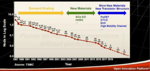
134
Best Quip of the Day
Dr. Y.-J. Mii, Senior Vice President of Research and Development /
Technology Development , highlighted three eras of process technology
development, as depicted in the figure below from his presentation.
In the first phase, Dennard scaling refers to the goal of scaling FEOL
linear lithographic dimensions by a factor of “s” (s < 1) in successive
process nodes, achieving an improvement of (1 / s**2) in circuit density,
measured as gates / mm**2. The next phase focused on material
improvements, and the current phase centers on design-technology co-
optimization – more on that shortly.
In a subsequent presentation at the symposium, Dr. Doug Yu, VP,
Integrated Interconnect and Packaging R&D, described how advanced
packaging technology has also been focused on scaling, albeit for a shorter
duration. “For over 10 years, packages have also offered two-dimensional
improvements to redistribution layer (RDL) and bump pitch lithography.
With the multi-die, 3D vertical stacking package technology we’re
describing today – specifically, TSMC’s SoIC offering—we are providing
vast improvements in circuit density. S is equal to zero. Or, in other words,

135
infinite scaling.” (Indeed, it is easy to foresee product technologies
starting to use the metric “gates / mm**3”.)
Here is a brief recap of the TSMC advanced process technology status.
N7/N7+
TSMC announced the N7 and N7+ process nodes at the symposium two
years ago. N7 is the “baseline” FinFET process, whereas N7+ offers
improved circuit density with the introduction of EUV lithography for
selected FEOL layers. The transition of design IP from N7 to N7+
necessitates re-implementation, to achieve a 1.2X logic gate density
improvement.
• N7 is in production, with over 100 new tapeouts (NTOs) expected
in 2019
• Key IP introduction: 112Gbps PAM4 SerDes
• N7+ is benefitting from improvements in sustained EUV output
power (~280 W) and uptime (~85%). “Although we anticipate
further improvements in power and uptime, these measures are
sufficient to proceed to N7+ volume ramp.”, TSMC said.
• TSMC has focused on defect density (D0) reduction for N7. “The
D0 improvement ramp has been faster than previous nodes, at a
comparable interval after initial production volume ramp.”,
according to TSMC.
• TSMC illustrated a dichotomy in N7 die sizes – mobile customers at
<100 mm**2, and HPC customers at >300 mm**2.
• To my recollection, for the first time TSMC also indicated they are
tracking D0 specifically for “large chips”, and reported a comparable
reduction learning for large designs as for other N7 products.
136
• N7+ will enter volume ramp in 2H2019, and is demonstrating
comparable D0 defect rates as N7.
“Making 5G a Reality”
TSMC invited Jim Thompson, CTO, Qualcomm, to provide his
perspective on N7—a very enlightening presentation:
• “N7 is the enabler for the 5G launch, as demonstrated in our Key
highlights include the latest Snapdragon 855 release.”
• “5G MIMO with 256 antenna elements supports 64 simultaneous
digital streams – that’s 16 users each receiving 4 data streams to a
single phone.”
• “Antenna design is indeed extremely crucial for 5G, to overcome
path loss and signal blockage. There are new, innovative antenna
implementations being pursued – in the end, it’s just math, although
complex math for sure.”
• “There’s certainly lots of skepticism about the adoption rate of 5G.
Yet 5G is moving much faster than 4G did – at a comparable point
in the rollout schedule, there were only 5 operators and 3 OEM
devices supporting 4G, mostly in the US and South Korea.
Currently, there are over 20 operators and over 20 OEM devices
focused on 5G deployment, including Europe, China, Japan, and
Southeast Asia.”
• “And, don’t overlook the deployment of 5G in applications other
than consumer phones, such as ‘wireless factory automation’.
Communication to/from industrial robots requires high bandwidth,
low latency, and extremely high availability. Consider the
opportunities for manufacturing flexibility in a wire-free
environment, enabled by 5G.”
137
N6
TSMC introduced a new node offering, denoted as N6. This node has
some very unique characteristics:
• Design rule compatible with N7 (e.g., 57 mm M1 pitch, same as N7)
• IP models compatible with N7
• Incorporates EUV lithography for limited FEOL layers – “1 more
EUV layer than N7+, leveraging the learning from both N7+ and
N5”
• Tighter process control, faster cycle time than N7 constraint
• Same EDA reference flows, fill algorithms, etc. as N7
• N7 designs could simply “re-tapeout” (RTO) to N6 for improved
yield with EUV mask lithography
• Or, N7 designs could submit a new tapeout (NTO) by re-
implementing logic blocks using an N6 standard cell library (H240)
that leverages a “common PODE” (CPODE) device between cells
for an ~18% improvement in logic block density
• Risk production in 1Q’20 (a 13 level metal interconnect stack was
illustrated)
• Although design rule compatible with N7, N6 also introduces a
unique feature—“M0 routing”
The figure below illustrates a “typical” FinFET device layout, with M0
solely used as a local interconnect, to connect the source or drain nodes of
a multi-fin device and used within the cell to connect common nFET and
pFET schematic nodes.
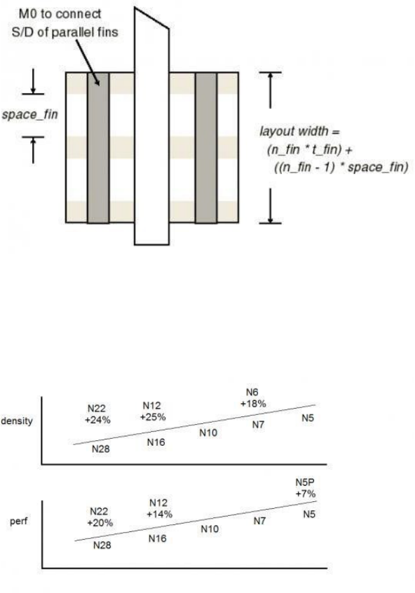
138
I need to ponder a bit more on the opportunity use M0 as a routing layer
– TSMC indicated that EDA router support for this feature is still being
qualified.
N6 strikes me as a continuation of TSMC’s introduction of a “half node”
process roadmap, as depicted below.
A half-node process is both an engineering-driven and business-driven
decision to provide a low-risk design migration path, to offer a cost-
reduced option to an existing N7 design as a “mid-life kicker”.
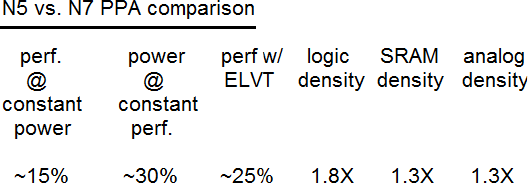
139
The introduction of N6 also highlights an issue that will become
increasingly problematic. The migration of a design integrating external IP
is dependent upon the engineering and financial resources of the IP
provider to develop, release (on a test site shuttle), characterize, and qualify
the IP on a new node on a suitable schedule. N6 offers an opportunity to
introduce a kicker without that external IP release
N5
The process node N5 incorporates additional EUV lithography, to
reduce the mask count for layers that would otherwise require extensive
multipatterning.
• Risk production started in March’19, high volume ramp in 2Q’20 at
the recently completed Gigafab 18 in Tainan (phase 1 equipment
installation completed in March’19)
• Intended to support both mobile and high-performance computing
“platform” customers; high-performance applications will want to
utilize a new “extra low Vt”(ELVT) device
• 1.5V or 1.2V I/O device support
• An N5P (“plus”) offering is planned, with a +7% performance boost
at constant power, or ~15% power reduction at constant perf over
N5 (one year after N5)
• N5 will utilize a high-mobility (Ge) device channel
140
Advanced Materials Engineering
In addition to the N5 introduction of a high mobility channel, TSMC
highlighted additional materials and device engineering updates:
• Super high-density MIM offering (N5), with 2X ff/um**2 and 2X
insertion density
• New low-K dielectric materials
• Metal Reactive Ion Etching (RIE), replacing Cu damascene for
• A graphene “cap” to reduce Cu interconnect resistivity
An improved local MIM capacitance will help to address the increased
current from the higher gate density. TSMC indicated an expected single-
digit % performance increase could be realized for high-performance (high
switching activity) designs.
Nodes 16FFC and 12FFC both received device engineering
improvements:
• 16FFC+ : +10% perf @ constant power, +20% power @
constant perf over 16FFC
• 12FFC+ : +7% perf @ constant power, +15% power @
constant perf over 12FFC
NTOs for these nodes will be accepted in 3Q’19.
TSMC also briefly highlighted ongoing R&D activities in materials
research for future nodes—e.g., Ge nanowire/nanoslab device channels,
2D semiconductor materials (ZrSe2, MoSe2)—see the figure below
(Source: TSMC).
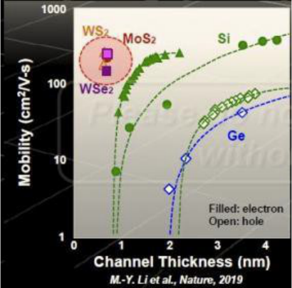
141
Manufacturing Excellence
Dr. J.K. Wang, SVP, Fab Operations, provided a detailed discussion of
the ongoing efforts to reduce DPPM and sustain “manufacturing
excellence”. Of specific note were the steps taken to address the demanding
reliability requirements of automotive customers. Highlights of Dr. Wang’s
presentation included:
“Since the introduction of the N16 node, we have accelerated the
manufacturing capacity ramp for each node in the first 6 months at an ever-
increasing rate. The N7 capacity in 2019 will exceed 1 million 12” wafers
per year. The N10/N7 capacity ramp has tripled since 2017, as phases 5
through 7 of Gigafab 15 have come online.”
“We have implemented aggressive statistical process control (measured
on control wafer sites) for early detection, stop, and fix of process
variations—e.g., upward/downward shifts in baseline measures, a variance
shift, mismatch among tools. We have established 2D wafer profile
measurement criteria, and in-line monitoring and comparison to an
“acceptance” profile across each wafer.”
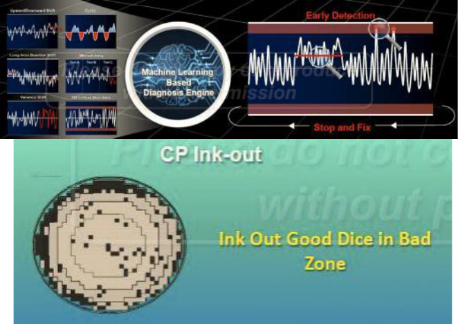
142
“The DDM reduction rate on N7 has been the fastest of any node.” “For
automotive customers, we have implemented unique measures to achieve
demanding DPPM requirements. We will ink out good die in a bad zone.
And, there are SPC criteria for a maverick lot, which will be scrapped.”
“We will support product-specific upper spec limit and lower spec limit
criteria. We will either scrap an out-of-spec limit wafer or hold the entire
lot for the customer’s risk assessment.” (See the figures below. Source:
TSMC)
Automotive Platform
TSMC has developed an approach toward process development and
design enablement features focused on four platforms – mobile, HPC, IoT,
and automotive. Dr. Cheng-Ming Lin, Director, Automotive Business
Unit, provided an update on the platform, and the unique characteristics of
automotive customers.
143
Growth in Semi Content
Dr. Lin indicated, “Automotive systems will require both advanced logic
technologies for ADAS, such as N16FFC, and advanced RF technologies
for V2X communications. Although the CAGR for cars from now to 2022
is expected to be only ~1.8%, the CAGR for the semiconductor content
will be 6.9%.”
He continued, “The L1/L2 feature adoption will reach ~30%, with
additional MCUs applied to safety, connectivity, and EV/hybrid EV
features. There will be ~30-40 MCU’s per vehicle. “ (In his charts, the
forecast for L3/L4/L5 adoption is ~0.3% in 2020, and 2.5% in 2025.) “The
adoption rate for the digital dashboard cockpit visualization system will also
increase, driving further semiconductor growth – 0.2% in 2018 to 11% in
2025.”
L2+
The levels of support for automated driver assistance and ultimately
autonomous driving have been defined by SAE International as “Level 1
through Level 5”. Perhaps in recognition of the difficulties in achieving L3
through L5, a new “L2+” level has been proposed (albeit outside of SAE),
with additional camera and decision support features.
“An L2+ car would typically integrate 6 cameras, 4 short-range radar
systems, and 1 long-range radar unit, requiring in excess of 50GFLOPS
graphics processing and >10K DMIPS navigational processing
throughput.”
N16FFC, and then N7
The 16FFC platform has been qualified for automotive environment
applications – e.g., SPICE and aging models, foundation IP
characterization, non-volatile memory, interface IP. The N7 platform will
be (AEC-Q100 and ASIL-B) qualified in 2020. "Automotive customers
tend to lag consumer adoption by ~2-3 years, to leverage DPPM learning
144
– although that interval is diminishing. We anticipate aggressive N7
automotive adoption in 2021,” Dr. Lin indicated.
“The TSMC RF CMOS offerings will be used for SRR, LRR, and Lidar.
The 16FFC-RF-Enhanced process will be qualified for automotive
platforms in 2Q’20.”
IoT Platform
The TSMC IoT platform is laser-focused on low-cost, low (active) power
dissipation, and low leakage (standby) power dissipation. Dr. Simon Wang,
Director, IoT Business Development, provided the following update:
Process Roadmap
• 55ULP, 40ULP (w/RRAM): 0.75V/0.7V
• 22ULP, 22ULL: 0.6V
• 12FFC+_ULL: 0.5V (target)
• Introduction of new devices for the 22ULL node: EHVT device, ultra-
low leakage SRAM
The 22ULL SRAM is a “dual VDD rail” design, with separate logic (0.6V,
SVT + HVT) and bitcell VDD_min (0.8V) values for optimum standby
power.
The 22ULL node also gets an MRAM option for non-volatile memory.
Note that a new methodology will be applied for static timing analysis for
low VDD design. The stage-based OCV (derating multiplier) cell delay
calculation will transition to sign-off using the Liberty Variation Format
(LVF).
The next generation IoT node will be 12FFC+_ULL, with risk
production in 2Q’20. (with low VDD standard cells at SVT, 0.5V VDD).
145
RF
TSMC emphasized the process development focus for RF technologies,
as part of the growth in both 5G and automotive applications. Dr. Jay Sun,
Director, RF and Analog Business Development provided the following
highlights:
• For RF system transceivers, 22ULP/ULL-RF is the mainstream
node. For higher-end applications, 16FFC-RF is appropriate,
followed by N7-RF in 2H’20.
• Significant device R&D is being made to enhance the device ft and
fmax for these nodes – look for 16FFC-RF-Enhanced in 2020
(fmax > 380 GHz) and N7-RF-Enhanced in 2021.
• New top-level BEOL stack options are available with ‘elevated’
ultra thick metal for inductors with improved Q.
• For sub-6 GHz RF front-end design, TSMC is introducing N40SOI
in 2019 – the transition from 0.18 um SOI to 0.13 um
SOI to N40SOI will offer devices with vastly improved ft and fmax.
Summary
There was a conjecture/joke going around a couple of years ago,
suggesting that “only 7 customers will be able to afford to pursue 7 nm
designs, and only 5 customers at 5 nm”. Clearly, the momentum behind
N7/N6 and N5 across mobile communication, HPC, and automotive (L1-
L5) applications dispels that idea. TSMC is investing significantly in
enabling these nodes through DTCO, leveraging significant progress in
EUV lithography and the introduction of new materials.
Reference: Tom Dillinger 2019 TSMC Technology Symposium Review
4/30/2019 www.semiwiki.com
147
2019 Update: Dr. Morris Chang
In 2017 the TSMC Museum of Innovation opened Under Fab 12 in
Hsinchu Taiwan. It not only commemorates the history of semiconductors
and TSMC but also the life of Dr. Morris Chang. Morris Chang’s wife
Sophie was actively involved in this project:
The TSMC Museum of Innovation encompasses three exhibition
galleries: "A World of Innovation,” "Unleashing Innovation," and "Dr.
Morris Chang, TSMC Founder." Through interactive technology, digital
content, and historical documents we will learn about the pervasiveness of
ICs in our daily lives and about their continued advancement. In addition,
we will learn how ICs are making our lives more fulfilling and how they are
driving technology beyond our imagination. We will also learn how TSMC
contributes to global IC innovation and to Taiwan's economy.
In 2018 Dr. Morris Chang retired from TSMC for the second and final
time:
TSMC Dr. Morris Chang Announces Retirement in June 2018.
Future Dual Leadership Will Be Mark Liu as Chairman And C.C.
Wei as CEO.
Issued by: TSMC Issued on: 2017/10/02
148
Hsinchu, Taiwan, R.O.C. – Oct. 2, 2017 – TSMC Chairman Morris Chang
today announces: “I will retire from the Company immediately after the Annual
Shareholders Meeting in early June, 2018. I will not be a director in the next term of
the board of directors. Nor will I participate in any TSMC management activities after
the Annual Shareholders Meeting in early June, 2018. From early June, 2018 on,
TSMC will be under the dual leadership of Dr. Mark Liu and Dr. C.C. Wei. Dr.
Mark Liu will be the Chairman of the Board, and Dr. C.C. Wei will be the Chief
Executive Officer. All present directors of the board have agreed to be nominated, and if
elected, serve as directors of the board during the next term. They have also agreed to
support the aforementioned dual leadership of the Company under Drs. Liu and Wei.
Chairman Morris Chang further said, “The past 30-odd years, during which I founded
and devoted myself to TSMC, have been an extraordinarily exciting and happy phase of
my life. Now, I want to reserve my remaining years for myself and my family. Mark and
CC have been Co-CEO’s of the Company since 2013 and have performed outstandingly.
After my retirement, with the continued supervision and support of an essentially
unchanged board, and under the dual leadership of Mark and CC, I am confident that
TSMC will continue to perform exceptionally.”

149
In Their Own Words:
GLOBALFOUNDRIES
GLOBALFOUNDRIES is the newest pure-play foundry in
the industry. In this chapter, GLOBALFOUNDRIES
describes its history, mission, and future directions.
The fabless semiconductor model, first implemented in the early 1980s
when IDMs figured out there was money to be made in selling excess
manufacturing capacity to small chip design companies, has been an
unqualified success in delivering innovation and efficiency to the
electronics industry. The emergence of ‘pure-play’ foundries in the mid-
1980s enhanced the model further still, and has enabled the success of
some of the most recognized and groundbreaking names in the
semiconductor industry—firms like Qualcomm, Broadcom, Marvel, Xilinx
and a host of others, not to mention forward-thinking product makers like
Apple and Microsoft.
Indeed, the days of “Real men own fabs” seem like a distant memory in
an era when a new manufacturing plant can cost more than $5 billion,
150
process technology is approaching sub 10 nm levels, and market windows
are measured in weeks not years.
As with all dynamic markets and business models, change is a constant
in how ICs are fabricated. While it’s fair to say that after 30 years, the
foundry model has withstood the test of time, it must evolve if it is to meet
the never-ending technology and economic challenges of the
semiconductor industry. The fact that mobile products surpassed PCs as
the largest consumer of semiconductors for the first time in 2012
underscores the macro changes that are reshaping the landscape of
electronics and forcing a re-thinking of the supply chain. Add in seemingly
inconceivable technology drivers and unfathomable price tags, and it’s clear
that those who can’t adapt to change in the semiconductor manufacturing
world are doomed.
It was against this backdrop that some visionaries dreamed of taking a
new approach to the foundry model as the first decade of the 21st Century
neared an end. After all, the foundry business itself hadn’t really changed
that much since its inception nearly 30 years prior, even if the pace of
technology evolution had maintained its steady march forward, driven by
the unceasing pace of Moore’s Law. So the reasoning was that there needed
to be some more significant enhancements of the model to better deal with
the challenges at hand. The industry needed a revamp, an upgrade, a new
release, and most importantly, a more global orientation—it needed
Foundry 2.0. GLOBALFOUNDRIES embodied the vision when it was
launched in March 2009.
Ironically, a cornerstone of the strategy centered on the very model that
foundries originally disaggregated: the integrated device manufacturer (IDM).
The founders of GLOBALFOUNDRIES recognized that there needed to
be a tighter connection between the design process —right from the
beginning at the architectural level—and the implementation in
manufacturing. The ‘throw it over the wall’ method of Foundry 1.0 was
151
breaking, and closer collaboration was viewed as the only way to deal with
the current challenges.
So it should be no surprise that a key aspect of the GLOBALFOUNDRIES
legacy can be traced back to one of the world’s leading IDMs. In October
2008, AMD announced a new strategy to focus exclusively on the design
phase of semiconductor product development. To achieve that strategy,
AMD partnered with Advanced Technology Investment Company (ATIC)
of Abu Dhabi to create a new joint venture company designed to become
the world’s first truly global foundry.
2009: The Birth of Foundry 2.0
On March 4, 2009, GLOBALFOUNDRIES officially launched as a new
joint venture, coupling AMD’s leading-edge semiconductor
manufacturing capabilities with the financial focus of ATIC, creating a new
global semiconductor manufacturing foundry with approximately 3,000
employees. This formally entered GLOBALFOUNDRIES in the foundry
business and armed it out of the gates with a production-proven fab
campus based in Dresden, Germany—and years of seasoned experience in
semiconductor design and manufacturing. AMD became its first customer.
Success with customers beyond AMD soon followed. Through the
course of 2009, the company announced several new customers and new
strategic partnerships, including ARM, STMicroelectronics, and
Qualcomm.
In June of that same year, GLOBALFOUNDRIES took the first step in
what was to become a defining element of its strategy. It was then that the
company broke ground on the Fab 8 campus, the company’s newest 300
mm fab in Saratoga County, New York. It was to be rightly heralded as the
most advanced semiconductor manufacturing facility ever constructed.
The Chartered Acquisition
In January 2010, the company announced the completion of its merger
with Chartered Semiconductor, a global semiconductor foundry company
152
based in Singapore. At the time, Chartered consisted of about 7,000
employees, mostly based at the company’s six fabs in Singapore. The
addition of Chartered added more than 150 customers to the company’s
portfolio, afforded world-class production capabilities in both mainstream
and leading-edge technologies and allowed the company to offer a new
platform for innovation to drive the current and future generations of
semiconductor products for customers around the globe.
Overnight, GLOBALFOUNDRIES had become one of the world’s top
3 foundries and the industry couldn’t help but take notice. The addition of
Chartered added proven experience in the workings of the foundry model,
complementing the IDM legacy from the company’s roots in AMD. In
addition, Chartered was skilled at the partnership model and
GLOBALFOUNDRIES found itself with a seat at the table of the ground-
breaking Common Platform Alliance, which included IBM and Samsung
in an initiative that defined new levels of collaboration among chip
manufacturers and customers. The Chartered acquisition also brought
with it much-needed capacity and a gateway into more application areas. The
Singapore operations would continue to play a major role in the company’s
strategy.
By 2011, GLOBALFOUNDRIES was hitting full stride, continuing to
add customers and reaching significant manufacturing milestones as
AMD’s 32 nm processor shipments increased by more than 80% from the
third quarter to the fourth quarter. In fact, GLOBALFOUNDRIES exited
2011 as the only foundry to have shipped in the hundreds of thousands of
32 nm high-K metal gate (HKMG) wafers.
New Leadership for a New Era
With the initial growing pains behind it, the company now was squarely
focused on growth and implementing its vision. To that end, Ajit Manocha
was named CEO of the company in late 2011. A skilled leader, he brought
more than 30 years of experience in the semiconductor industry, having
held senior positions at Spansion, NXP, and AT&T Microelectronics.
153
Manocha was a safe pair of hands to bring the company to the next stage.
Manocha understood the value of partnerships and collaboration well and
quickly wove that philosophy deeper into the fabric of the company.
Collaborative Device Manufacturing (CDM) became the new mantra for
the model GLOBALFOUNDRIES espoused, under the name Foundry
2.0, and brand name customers and partners from around the ecosystem
embraced it. In January 2014, Sanjay Jha was appointed CEO and Manocha
returned to his role advising the owners of GLOBALFOUNDRIES. Jha’s
background was in mobile, with a long tenure at Qualcomm and a period
as CEO of Motorola Mobility.
Mobile is, of course, the largest market for semiconductors today and
continues to grow fast.
Global Leadership at the Leading Edge
Unique to the foundry industry, GLOBALFOUNDRIES operates a
global network of advanced manufacturing and technology capabilities,
anchored by 300 mm and 200 mm facilities in Singapore, Germany, and
the company’s newest campus in Saratoga County, New York. Periodic
benchmarking conducted by third parties consistently places
GLOBALFOUNDRIES as a leader worldwide in the major categories for
fab performance. This advanced network of manufacturing campuses and
global research partnerships provides the company the ability to introduce
technologies with greater process maturity than is typical of the foundry
industry, enabling the fastest volume ramps in the industry.
Fab 1: Dresden
The Dresden manufacturing site is recognized throughout the industry
as among the most successful leading-edge semiconductor production
facilities in the world. Fab 1 represents one of the biggest international
investments in Germany with a total investment to date of more than $7
billion, and about 3,000 world-class engineers, technicians, and specialists.
154
Fab 7: Singapore
GLOBALFOUNDRIES has two manufacturing campuses in Singapore
with four 200 mm wafer fabrication plants (Fab 2, 3/5, 6) and one 300 mm
wafer fabrication plant (Fab 7) located in Woodlands and another 200 mm
manufacturing facility (Fab 3E) in Tampines.
The Singapore site is embarking upon a long-term strategic plan to focus
on upgrading the manufacturing facilities to address fast-growing “More
Than Moore” technology areas such as MEMS, RF and analog/ mixed
signal with technology nodes spanning from 180 nm to 40 nm.
Fab 8: New York
For more than two decades, the focus of the semiconductor foundry
industry has increasingly turned to Asia for growth and the development
of new manufacturing facilities. Counter to this prevailing trend, the Fab 8
project is the first leading-edge semiconductor foundry to be built in the
U.S. and one of the largest new manufacturing projects in the world. The
project is a key driver in the revitalization of upstate New York’s “Tech
Valley” and a prime example of how advanced manufacturing can help
boost the American economy. Building on a history of award-winning
manufacturing facilities, GLOBALFOUNDRIES is developing the world’s
most advanced semiconductor wafer fab at the Luther Forest Technology
Campus in upstate New York.
Less than 3 years since its formation, the company’s multi-billion dollar
investment in upstate New York and its extensive network of partnerships
in that region began to bear fruit in 2012. In January of that year,
GLOBALFOUNDRIES started running first customer silicon at Fab 8
with IBM’s 32 nm SOI technology. This technology was jointly developed
between GLOBALFOUNDRIES and other members of IBM’s Process
Development Alliance, including early-stage research at the University of
Albany, State University of New York’s College of Nanoscale Science and
Engineering.
155
In July 2012, GLOBALFOUNDRIES announced an extension of
90,000 square feet to the Fab 8 Module 1 cleanroom in response to strong
customer demand at the 28 nm node. The extension of Fab 8 increased the
cleanroom to approximately 300,000 square feet, roughly equivalent to six
football fields of state-of-the-art semiconductor wafer manufacturing
space. Construction work on the Fab 8 Module 1 extension project began in
September and is expected to be completed in December 2013.
Technology innovation, through partnerships and extensive investment in
R&D, continues to make GLOBALFOUNDRIES a force to be reckoned
with. The company has established itself among the industry’s elite,
aggressively laying out a roadmap to 10 nm and beyond. It delivered on its
promises with the announcement of the industry’s first modular 14 nm
offering, a breakthrough FinFET approach specifically aimed at the
burgeoning opportunities in mobile application markets. This was a
reflection of an acceleration of its leading-edge roadmap to give customers
the performance and power benefits of three-dimensional FinFET
transistors with less risk and faster time-to-market.
In addition, GLOBALFOUNDRIES began ramping its 20 nm
technology in 2012, and saw significant adoption and yield improvements
for its 28 nm offerings. By year end, it was clear the company no longer
would take a back seat to anyone when it comes to technology.
The Emergence of a True Market Leader
By mid-2012, GLOBALFOUNDRIES had surpassed its nearest
competitor and was firmly established as the world’s second largest foundry
in the industry rankings. The company was buoyed by the continued
growth of the foundry market in general, and its unique application of the
model was winning new customers at an impressive rate.
An IC Insights report in 2012 was especially significant for
GLOBALFOUNDRIES as the company jumped six spots to break into
the top 20 IC companies for the first time, and IC Insights projects its
revenue to grow 31% over 2011, making GLOBALFOUNDRIES the
156
fastest growing semiconductor company in the world. The firm sang the
praises of GLOBALFOUNDRIES approach, noting, “It is obvious that
GLOBALFOUNDRIES’ current spike in revenue is being driven mostly
by its success in attracting new IC foundry customers.”
Focus on Collaborative Technology Development
In January 2013, GLOBALFOUNDRIES announced a new global R&D
facility at its Fab 8 campus. The new Technology Development Center
(TDC) Technology Development Center will play a key role in the
company’s strategy to develop innovative semiconductor solutions
allowing customers to compete at the leading edge of technology.
The TDC will house a variety of semiconductor development and
manufacturing spaces to support the transition to new technology nodes,
as well as the development of innovative capabilities to deliver value to
customers beyond the traditional approach of shrinking transistors. The
overarching goal of the TDC is to provide a collaborative space for
GLOBALFOUNDRIES to develop end-to-end solutions covering the full
spectrum of silicon technology, from new interconnect and packaging
technologies that enable three-dimensional (3D) stacking of chips to
leading-edge photomasks for Extreme Ultraviolet (EUV) lithography and
everything in between.
The TDC represents an additional investment of nearly $2 billion,
increasing the total capital investment for the Fab 8 campus to
approximately $8 billion. Construction of the TDC began in early 2013 and
is expected to be completed in late 2014.
With the addition of Fab 8, GLOBALFOUNDRIES now operates three
300 mm wafer fabs around the world with campuses in Germany,
Singapore and New York offering customers leading-edge volume
manufacturing capabilities at the 32 nm and 28 nm process nodes and
technology development at 20 nm, 14 nm and beyond. In addition,
GLOBALFOUNDRIES also operates five 200 mm wafer fabs in
157
Singapore, offering global customers a broad spectrum of manufacturing
technology options.
Foundry 2.0 Today and for the Future
Most industry watchers have confirmed that GLOBALFOUNDRIES is
a first-of-its-kind global foundry model, bringing a unique approach to
leveraging assets from around the world to best meet the needs of the
global marketplace. Since its inception the company has made substantial
capital investments to build a truly global footprint, with manufacturing
operations spanning three continents for flexible and secure supply. Today
it employs more than 13,000 people worldwide, and with manufacturing
centers in Germany, the United States and Singapore,
GLOBALFOUNDRIES is delivering advanced technologies to market in
high volume and mature yield faster than any other foundry in the world.
This global manufacturing footprint is supported by major facilities for
research, development, and design enablement located across the U.S.,
Europe, and Asia, with offices in Abu Dhabi and corporate offices in
Silicon Valley. The collective strength of these operations is unprecedented
for a semiconductor foundry and unparalleled in the industry.
A final, perhaps symbolic, milestone was reached in 2013 when AMD
completed its divestiture of the remaining 14% stake it had in
GLOBALFOUNDRIES. The transition from IDM to foundry was now
complete. Just four short years from its founding, GLOBALFOUNDRIES is
wholly owned by ATIC and is firmly entrenched as the world’s second
largest independent semiconductor foundry that has written an entirely new
chapter in the history of an industry.
159
2019 Update: GLOBALFOUNDRIES
The GLOBALFOUNDRIES story has been one of the more interesting
ones inside the fabless semiconductor ecosystem. It started in 2008 when
AMD announced a partnership with ATIC of Abu Dhabi to create a new
joint venture company and become the world’s first truly global
semiconductor foundry. On March 4th of 2009 GLOBALFOUNDRIES
was launched and the rest as they say is history. It has been an exciting story
to cover, absolutely.
GF had a rough start due in part to a shift in the foundry landscape.
TSMC made a series of technology changes that made it difficult for others
to follow. It all started at 28 nm. While most foundries chose the gate-first
implementation TSMC chose gate-last. As it turned out the gate-first
implementation did not yield properly which gave TSMC their largest
process node lead ever. UMC and SMIC ended up changing to gate-last to
copy TSMC and get second-source manufacturing market share but
Samsung and GF stayed with gate-first. Then came FinFETs which made
following TSMC for second source business impossible. Samsung did a
very nice job with 14 nm which resulted in a 50/50 split market share with
TSMC 16 nm but TSMC quickly came back with 10 nm and 7 nm and is
now in a dominant FinFET foundry position.
This caught GF in between two fierce competitors (TSMC and Samsung)
which is an impossible place to be in the foundry business, even for a chip
giant like Intel. The end came in 2018 when both Intel and GF decided to
step aside and let TSMC and Samsung battle for the leading-edge foundry
160
business. The GF pivot is still in process and it does include asset sales.
Here is the original press release:
GLOBALFOUNDRIES Reshapes Technology Portfolio to
Intensify Focus on Growing Demand for Differentiated Offerings
Semiconductor manufacturer realigns leading-edge roadmap to meet
client need and establishes wholly owned subsidiary to design custom
ASICs
Santa Clara, Calif., August 27, 2018 – GLOBALFOUNDRIES today
announced an important step in its transformation, continuing the
trajectory launched with the appointment of Tom Caulfield as CEO earlier
this year. In line with the strategic direction Caulfield has articulated, GF is
reshaping its technology portfolio to intensify its focus on delivering truly
differentiated offerings for clients in high-growth markets.
GF is realigning its leading-edge FinFET roadmap to serve the next wave
of clients that will adopt the technology in the coming years. The company
will shift development resources to make its 14/12 nm FinFET platform
more relevant to these clients, delivering a range of innovative IP and
features including RF, embedded memory, low power and more. To
support this transition, GF is putting its 7 nm FinFET program on hold
indefinitely and restructuring its research and development teams to
support its enhanced portfolio initiatives. This will require a workforce
reduction; however a significant number of top technologists will be
redeployed on 14/12 nm FinFET derivatives and other differentiated
offerings.
“Demand for semiconductors has never been higher, and clients are
asking us to play an ever-increasing role in enabling tomorrow’s technology
innovations,” Caulfield said. “The vast majority of today’s fabless
customers are looking to get more value out of each technology generation
to leverage the substantial investments required to design into each
technology node. Essentially, these nodes are transitioning to design
161
platforms serving multiple waves of applications, giving each node greater
longevity. This industry dynamic has resulted in fewer fabless clients
designing into the outer limits of Moore’s Law. We are shifting our
resources and focus by doubling down on our investments in
differentiated technologies across our entire portfolio that are most
relevant to our clients in growing market segments.”
In addition, to better leverage GF’s strong heritage and significant
investments in ASIC design and IP, the company is establishing its ASIC
business as a wholly-owned subsidiary, independent from the foundry
business. A relevant ASIC business requires continued access to leading-
edge technology. This independent ASIC entity will provide clients with
access to alternative foundry options at 7 nm and beyond, while allowing
the ASIC business to engage with a broader set of clients, especially the
growing number of systems companies that need ASIC capabilities and
more manufacturing scale than GF can provide alone.
GF is intensifying investment in areas where it has clear differentiation
and adds true value for clients, with an emphasis on delivering feature-rich
offerings across its portfolio. This includes a continued focus on its
FDXTM platform, leading RF offerings (including RF SOI and high-
performance SiGe), analog/mixed-signal, and other technologies designed
for a growing number of applications that require low power, real-time
connectivity, and on-board intelligence. GF is uniquely positioned to serve
this burgeoning market for “connected intelligence,” with strong demand
in new areas such as autonomous driving, IoT and the global transition to
5G.
“Lifting the burden of investing at the leading edge will allow GF to make
more targeted investments in technologies that really matter to the majority
of chip designers in fast-growing markets such as RF, IoT, 5G, industrial
and automotive,” said Samuel Wang, research vice president at Gartner.
“While the leading edge gets most of the headlines, fewer customers can
afford the transition to 7 nm and finer geometries. 14 nm and above
162
technologies will continue to be the important demand driver for the
foundry business for many years to come. There is significant room for
innovation on these nodes to fuel the next wave of technology.”
About GF
GLOBALFOUNDRIES is a leading full-service semiconductor foundry
providing a unique combination of design, development, and fabrication
services to some of the world’s most inspired technology companies. With
a global manufacturing footprint spanning three continents,
GLOBALFOUNDRIES makes possible the technologies and systems that
transform industries and give clients the power to shape their markets.
GLOBALFOUNDRIES is owned by Mubadala Investment Company. For
more information, visit www.globalfoundries.com.
If you look at GF there are five different semiconductor business units:
Singapore fabs, Dresden fabs, the Malta fab, IBM fabs, and the new fab in
China.
One of the Singapore fabs (MEMs Fab 3e) has been sold to VIS in
Taiwan (January 2019). TSMC is a major shareholder in VIS and already
one of the top MEMs manufacturers. The other Singapore fabs are
rumored to be up for sale as well.
The Malta fab has NY State funding and is currently running Samsung
14 nm technology so Samsung is a strong acquisition candidate. Samsung
already has a fab in Austin, Texas but adding another fab in NY would not
be a bad thing for US foundry customers. It is also possible for GF to
migrate Malta to FD-SOI when extra capacity is needed.
The Dresden fabs are probably the most desirable since they are leading
edge FD-SOI but again government funding is involved. If the German
government were forward-looking, they would take an active role in their
semiconductor future and embrace GF Dresden. Even so, Dresden seems
to be the jewel in the GF fab crown moving forward especially now that
GF has reportedly moved advanced mask making tools from Vermont to
163
Dresden. The China fab in Chengdu is also FD SOI so I would put it right
next to Dresden in the crown jewels.
Last but not least, the IBM fabs (Essex Junction and Fishkill) which were
part of the acquisition of IBM Microelectronics in July of 2015.
The Fishkill fab was sold to ON Semiconductor for $430 million in April
of 2019. The Essex Junction fab may be more difficult to sell due to the
age of the facility which was originally built in 1958. The Mask shop that
was part of Essex Junction fab was moved to Dresden in February of 2019.
Here is a more detailed description of the GF Pivot by Scott Jones of IC
Knowledge as published on www.semiwiki.com:
GLOBALFOUNDRIES Pivot Explained
GLOBALFOUNDRIES (GF) recently announced they were
abandoning 7 nm and focusing on “differentiated” foundry offerings in a
move our own Dan Nenni described as a “pivot”, a description GF appears
to have embraced. Last week GF held their annual Technology Conference
and we got to hear more about the pivot from new CEO Tom Caulfield
including why GF abandoned 7 nm and what their new focus is.
Background
GF was created in 2008 in a spin-out of the fabs formerly owned by
AMD. In 2010 GF acquired Chartered Semiconductor, the number three
foundry in the world at that time and in 2015 GF acquired IBM’s
microelectronics business. Figure 1 illustrates the key milestones in GF’s
history.
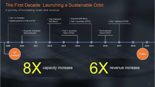
164
Figure 1. GLOBALFOUNDRIES Milestones.
GF is owned by Mubadala Development Company (MDC). MDC
financials include the technology segment made up of GF. Based on
Mubadala financial disclosures, from 2016 to 2017 GF grew revenues by
12.4% and saw their operating loss widen from 8.0% of revenue in 2016 to
27.2% of revenue in 2017 calling into question the sustainability of GF’s
business model.
On March 9
th
, 2018 Tom Caulfield became the new CEO of GF with a
mandate to build a sustainable business model.
7 nm History
In the early 2010s GF was developing their own 14 nm process
technology but realizing they were falling behind their competitors
ultimately abandoned their in-house development and licensed 14 nm from
Samsung. The licensed 14 nm process was launched in 2014 in Fab 8 (see
figure 1). GF has continued to improve on that process adding process
options and more recently launching a shrunk 12 nm version. The 14 nm
and newer 12 nm version have been utilized by AMD for microprocessors
165
and graphics processors, by GF for their FX-14 ASIC platform and by
other customers.
With the IBM Microelectronics acquisition in 2015, GF received a
significant infusion of researchers including Gary Patton who became the
CTO of GF. Beginning around 2016, the combined GF and IBM research
teams started to develop their own in-house 7 nm technology. The initial
version was planned to be based on optical exposures with GF also
planning an EUV based follow-on version.
By all account’s development was proceeding well. In a July 2017
SemiWiki exclusive, GF disclosed their key 7 nm process density metrics
and at IEDM in December 2017 GF disclosed additional process details.
One concern I have had about GF 7 nm for a long time is scale. GF was
reportedly installing only 15,000 wafers per month (wpm) of 7 nm capacity.
The average 300 mm foundry fab had 34,213 wpm capacity at the end of
2017 and are projected to reach over 40,343 wpm by the end of 2020, and
43,584 wpm by the end of 2025 [1]. Newer leading-edge fabs are even larger
and are what is driving up the average. At the leading-edge, wafer cost is
roughly 60% depreciation and larger fabs have better equipment capacity
matching and therefore higher capital efficiency and lower costs. Figure 2
illustrates the wafer cost versus fab capacity for a wafer fab in the United
States running a 7 nm process calculated using the IC Knowledge –
Strategic Cost and Price Model – 2018 – revision 03 for a greenfield fab.
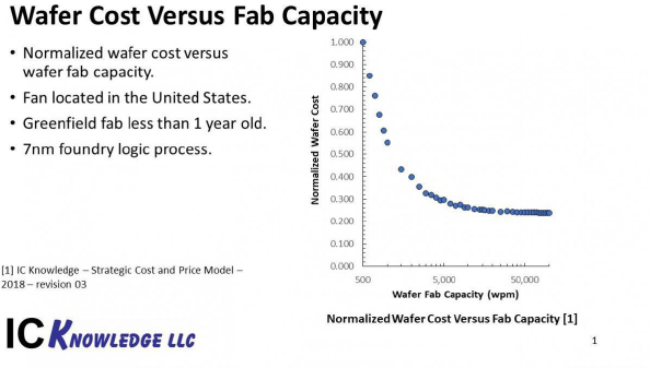
166
Figure 2. Wafer Cost Versus Fab Capacity for 7 nm Fab in the United States
Even though 15,000 wpm is past the steepest part of the curve there is
still several hundred dollars in cost per wafer advantage for larger capacity
wafer fabs.
Tom Caulfield also mentioned GF needed $3 billion dollars of additional
capital to get to 12,000 wpm and they could only fund half of it through
cash flow, they would have to borrow the other half and the projected
return wasn’t good.
Customer Inputs
When Tom took over as CEO he went out on the road and visited GF’s
customers. What he found was a lack of commitment to GF’s 7 nm process
in the customer base. Many customers were never going to go to 7 nm and
of the customers who were, GF wouldn’t have enough capacity to meet
their demands. There was also concern in the customer base that 7 nm
would take up all the R&D and capital budgets and starve the other
processes they wanted to use of investment.

167
What Did GF Give Up?
By exiting the 7 nm and smaller wafer market GF has given up some
opportunity. Figure 3 illustrates the total available market (TAM) for
foundry wafers in 2018 and 2022. Even in 2022 the forecast is for 7 nm to
be less than 25% of the market and the TAM for >=12 nm to increase
from $56 billion dollars in 2018 to $65 billion dollars in 2022.
Figure 3. Foundry market.
In terms of specific markets, GF is conceding some of the computing,
graphics processing and data center opportunity. Currently AMD is GF’s
largest customer and long term that business will presumably shrink as
AMD moves to smaller geometries.
What Now?
GF will be focused on four major “differentiated, feature-rich” offerings
going forward.
168
FinFET – GF will continue to offer 14 nm and 12 nm FinFET based
processes and they are continuing to add to these offerings with RF and
analog capabilities, improved performance (10-15%) and density (15%),
embedded memory options, enhanced MIM capacitors and advanced
packaging options.
RF – this is a segment where GF has a clear leadership position.. With
the pivot away from 7 nm, GF is increasing investment in this segment with
more capacity. At the Technology Conference GF said, “If you think RF,
think GF” and I agree that is an apt slogan.
FDSOI – GF’s FDX processes with 22FDX currently and 12FDX are
the industry leader in the emerging FDSOI space as I discussed in another
recent article available here. FDSOI shows great potential in the IOT and
Automotive markets. If FDSOI really takes off this could be a huge win
for GF and they have already announced $2 billion dollars of design wins
for the 22FDX process.
Power/AMS (Power. Analog and Mixed Signal) – this segment combines
Bipolar/CMOS/DMOS (BCD), RF, mmWave, embedded non-volatile
memory and Micro-Electro-Mechanical-Systems (MEMS) for the
consumer space such as high-speed touch interfaces.
Conclusion
GFs’s pivot away from 7 nm has aligned the companies R&D and capital
spending more closely with their customer’s needs. Whether GF can build
a sustainable business model on the four business segments they are now
focused on remains to be seen but more closely aligning your companies
focus with your customers’ needs certainly appears to be a step in the right
direction.
169
Chapter 6: Electronic Design
Automation
There is no doubt that EDA has been a key enabler of the fabless
semiconductor industry. EDA and IP are not so much the tail that wags
the dog, rather they are like the heart of an elephant, tiny in comparison
but without which there is no elephant. In this chapter, we lay out
(manually, as it turns out), the history of EDA as we see it, taking you
through the five historical phases of semiconductor design.
EDA, Phase One
From the earliest days of integrated circuits until the mid-1970s, chips
were designed manually, with no automation of any part of the design,
layout, verification, or mask preparation. The masks used for
photolithography were actually hand cut with X-ACTO knives out of a self-
adhesive red plastic film called Rubylith. Rubylith is no longer used in IC
manufacture, but it is still used to make masks in many other areas of
graphic design. When it was still used in IC design, the Rubylith was stuck
onto transparent paper or plastic in patterns that defined the transistors
and interconnect and then photoreduced to get the actual masks. As chips
got larger, this process became more and more unwieldy, both because of
the number of pieces of Rubylith required and because of the sheer size of
the sheets onto which it was stuck. It became clear that some method of
automation would be required very soon.
170
About this time, in the mid-1970s, three companies entered the market
for IC layout automation—Calma, Applicon, and ComputerVision. We
consider this the first phase of the EDA industry. Their products replaced
manual design layout with a computer system that allowed layout engineers
to trace out the mask shapes on the screen. When the design was released
to manufacturing, the software would save the layout to a magnetic tape
that a photoplotter could use to create the actual mask. This process was
called tape-out. Even though tapes are obsolete, and photoplotters have
been replaced with e-beam mask-making machines, releasing a design to
manufacturing is still called tape-out. Tape-out is the culmination of
months or even years of work. It is the point-of-no-return; a multi-million
dollar wager that every “T” has been crossed and every “I” dotted.
The complexity of chips has long demanded the use of computer
software to simulate chip behavior, design the physical layout of the chip,
verify the functionality, and ensure the design can be manufactured. The
broad and enormously sophisticated software programs that enable the
creation of all chips fall into the category of EDA software.
The original EDA companies (Calma, Applicon, and ComputerVision)
sold the hardware for the graphical layout with the software bundled in.
Because of this, the EDA industry business model was based on a hardware
business model—the customer purchased the hardware and paid an annual
maintenance charge to keep it running. This remained the model for the
EDA industry for many years, even after it became a pure software
business. There was even, for a time, a worry that the falling price of
hardware would pull the price of software down too, because software was
often bundled with hardware. In the 1970s, unlike today, software was
cheaper than hardware. As the relative value of hardware and software
inverted, the EDA industry worried that their customers would not pay
more for software than for the hardware on which it ran. Today this would
strike people as comical because computer hardware is a commodity and
EDA software (and other enterprise software like databases) costs
hundreds of times more.
171
Until about 1980, semiconductor design was only done inside
semiconductor companies. They decided what to make, then systems
companies could buy those chips and design products around them. Apart
from layout tools and some circuit simulation, most other software design
tools were largely developed in-house by internal computer-aided design
(CAD) groups.
For example, Hewlett-Packard created its own “integrated graphics
system” called HP-IGS. Long-time industry insider, Randy Smith, who’s
first EDA job was working on the HP-IGS, says the application software
ran on an HP3000 computer (really a 6-foot tall business computer) while
the graphics were processed and displayed on an HP1000 microcomputer.
Increasing the level of automation was seen to be a competitive
advantage and a company’s internal software was considered part of their
“secret sauce.” But the world was about to change, and the initial catalyst
for that change was largely a single, very influential, book.
EDA, Phase Two
In 1980, Carver Mead at Caltech and Lynn Conway at Xerox Palo Alto
Research Center (PARC) published their Introduction to VLSI Systems. This
book marked the first time that the details of designing an integrated circuit
were openly available to people outside of the semiconductor companies
themselves. Universities, research centers, and system companies could
suddenly consider designing their own integrated circuits rather than
buying chips from the semiconductor companies. Although chips at the
time could contain about 5,000 gates, which was too small to make most
interesting systems, the basic idea of Moore’s Law, that the number of gates
would double every couple of years, was by then well understood and its
implications were becoming clear. Semiconductor technology would grow,
and it would affect our lives in ways that were open to discovery. Any
electronic system could eventually be implemented with just a few chips,
and very inexpensively.
172
After the publication of Introduction to VLSI Systems, computer scientists
flocked to integrated circuit design. Unlike the VLSI designers in the
semiconductor companies, who often had a deep understanding of
electrical engineering and semiconductor process, the computer scientists
did what came naturally: they created simplified abstractions, specifically
hierarchy, to manage the complexity of chip design. The old ways of
designing, even with computer-aided layout on systems like Calma, could
not keep up with the growing complexity of designs with thousands of
gates, let alone the tens or hundreds of thousands that was anticipated
based on the Moore’s Law projections.
These abstractions created by the influx of computer scientists drove one
of the most important evolutions for the semiconductor industry— the
creation of ASICs, the chips designed for a specific use, as opposed to the
all-purpose chips that the semiconductor companies were creating at the
time.
As we mentioned in the ASIC chapter, the ASIC companies initially
produced many of their own design tools, but as the design processes
became more standardized, a more generic ASIC methodology emerged.
The ASIC flow essentially split the process into two distinct parts—front-
end and back-end. The front-end design was, and is still, done by the
systems companies and included the chip architecture and simulation. The
system company would select a library of standard cells for the design and
specify how to hook them up by using a special graphical software tool.
(Standard cells are a group of transistors that perform a logic or storage
function, implemented as fixed-height elements.)
The systems companies used simulation software to ensure that the
design performed as intended. This combination of library cells and how
they were interconnected, called the netlist, was then shipped to the ASIC
company who would do the physical design of the chip, also known as
back-end design.
173
Because the initial ASIC methodology split the design into two parts—
the front-end done at the systems company and the backend done at the
semiconductor company—two distinct types of EDA companies
flourished, and is the industry we still have today.
So, at this point, the industry had a design flow that was bifurcated into
front-end and back-end, and chips that continued to grow in complexity.
Both of these factors led to increased specialization of all aspects of the
ASIC flow and opened the door for a new crop of EDA companies—
Daisy Systems, Mentor Graphics, and Valid Logic Systems.
All three created tools to handle the front-end design tasks, mainly
schematic editing and simulation. Daisy and Valid continued the existing
Calma business model of selling hardware on which their software ran.
Mentor Graphics however, created software that ran on workstations made by
the company Apollo (who would be purchased by Hewlett-Packard in
1989). In the early days, all three provided roughly equivalent software for
schematic capture and for verifying designs through simulation.
The back-end design started with the netlist, timing information, and
process information. The placement of standard cells and the signal routing
between them was accomplished with the help of software developed in-
house by some ASIC companies or by one of the EDA companies—such
as Silvar-Lisco and Tangent Systems—that specialized in the hard-to-
master placement and routing algorithms.
None of the original big three layout companies—Calma, Applicon, or
ComputerVision—made the transition to this new world of ASIC in which
schematic design and automated place and route, as opposed to manual
layout, became the key enabling technologies. They were each eventually
absorbed into other companies and all the technologies they developed,
except for one, fell into the trash bin of history.
The one technology that did not vanish was Calma’s, called simply the
Graphic Design System or GDS, which they originally released in 1971.
The second version of it, introduced in 1978, was thus called GDSII. Back
174
in those days, computer hard drives couldn’t hold all the designs in progress,
nor was there good networking between systems, so design data was kept
on a magnetic tape in the GDSII stream format. This was essentially a daily
back up format. The layout designer would work on the design, then she
(many layout designers were women) would save it to the disk of a free
system. This GDSII format became the de facto standard for moving
design data around between systems. Amazingly, almost 40 years later, that
format is only just starting to be superseded (by a new standard called
OASIS) as the standard format for moving design layout between tools or
between design house and mask shop.
By late 1980s, a lot of semiconductor design was done using the ASIC
methodology, with the system companies doing the front-end and the
semiconductor companies doing the back-end physical design. This was
the second phase of the EDA industry.
EDA, Phase Three
The third phase of the EDA industry was driven by two factors. Firstly, it
became unfeasible for every semiconductor company to develop all their
own place and route tools internally, so more and more companies
discontinued their internal development in favor of buying EDA tools from
external EDA companies. Secondly, it became possible for system
companies to do their own back-end design in addition to the front-end,
so they didn’t rely as heavily on ASIC companies to complete the physical
layout of their designs.
These two trends meant that the EDA industry no longer focused just
on the front-end where Daisy, Mentor and Valid were strong, but began to
focus on products for the more complex physical design.
The most important company of this third phase of the EDA industry
was Cadence Design Systems. In fact, Cadence was created as the merger
of two earlier companies, SDA and ECAD, who produced tools for
physical layout and tools for verifying that they were laid out correctly.
175
Cadence became the dominant company for custom design, and following its
acquisition of Tangent Systems in 1989, also for place and route.
Just as Calma, Applicon, and ComputerVision vanished at the start of
the second phase of the EDA industry, Daisy, Mentor, and Valid were
overtaken by the new EDA companies like Cadence. Daisy made an unwise
merger with Cadnetix Corp in 1988 and soon after went out of business.
As an interesting side note, the defunct Daisy was picked up in 1990 by
Intergraph Corp, which had been the parent corporation of Tangent before
Tangent was acquired by Cadence the year before. Cadence also acquired
Valid in 1992. Intergraph used Daisy/Cadnetix technology in their new
subsidiary called VeriBest, who was acquired by Mentor in 1999. Got all
that? Of the three, only Mentor survived intact, but it spent years re-
architecting itself for the new era and only in recent years has it acquired a
full portfolio of physical design and verification tools.
There were two other companies that were significant during this third
phase of the industry—Gateway Design and Arcsys. Gateway created the
simulation language called Verilog and produced a high-performance
simulator. Cadence acquired them in 1989 for $72 million, which at the
time, seemed an enormous price. In hindsight, it is one of the most
successful EDA acquisitions ever. Verilog turned out to be extremely
important in the fourth phase of the EDA industry.
Arcsys was created to compete with Cadence in automatic place and
route, which was then the biggest and richest sub-segment of the EDA
industry. Arcsys acquired a physical verification company called Integrated
Silicon Systems (ISS) in 1995 and changed its name to Avant! (pronounced
“ah-VAHN-tee”). They became the second company behind Cadence in the
physical design area.
Arcsys/Avant! became infamous for another reason: its first product was
built on source code for the underlying database that was stolen from
Cadence. This led to FBI raids and years of litigation before both the
176
criminal and civil processes eventually concluded with jail terms and
hundreds of millions of dollars in restitution and fines.
EDA, Phase Four
So the third phase of the EDA industry saw semiconductor companies
replacing their internal tools by, largely, Cadence and Avant! software. The
fourth phase of the EDA industry was the transition to synthesis-based
design, which only became mainstream in the mid-1990s. Graphical
schematic-based design was replaced, except for analog and some other
specialized areas, by language-based synthesis with astounding leaps in
design productivity. Synopsys won this part of the market but there were
many competing technologies in the beginning: SILC, Autologic, Trimeter,
and others. Much later, Cadence tried to develop its own synthesis product,
called Synergy, but it was never successful.
Synopsys built their logic synthesis business in stages. First they created
logic optimization products that took the netlists from graphical schematic
capture and improved them. Then they produced a tool that would read
Verilog, automatically create a netlist that had the same functionality, then
optimize it. This synthesis-based approach to design is still the mainstream
today, and the synthesis tools have improved in performance, capacity and
other dimensions.
Around 1998, at the end of this fourth phase of the EDA industry, the
landscape was as follows: in custom design Cadence was dominant; in place
and route the market was split between Cadence and Avant!; in simulation
Mentor, Cadence, and Synopsys had products, but Synopsys was dominant;
in physical verification Cadence led, but Avant! and Mentor both had
products too.
EDA, Phase Five
The fifth phase of the EDA industry, which brings us up to the present
time, is the era of full-service EDA companies. Through the mid-1990s,
most semiconductor companies built their design flow with point tools for
177
each stage of the design flow, regardless of how many EDA vendors they
had to buy from. This strategy grew out of necessity because no one EDA
company had all the tools they needed. Synopsys and Mentor had no place
and route, and Cadence had no synthesis, for example. It was impossible to
put a whole flow together from one EDA company.
In pursuit of full-flow software offerings, Cadence acquired synthesis
technology from the companies Ambit in 1998 and Get2Chip in 2003.
Synopsys acquired Avant! in 2001, thus concluding Avant!’s legal woes.
Mentor was slower to round out its offerings by finding place and route
tools, but it made up for it when, almost overnight, its Calibre physical
verification software replaced Cadence’s product (Dracula) as the industry
standard.
As EDA companies built portfolios of software to cover the entire design
flow, semiconductor companies switched from putting together their own
flows with best-in-class point tools from a mixture of companies, to picking
a single primary supplier, typically Cadence or Synopsys, and supplementing
with some additional tools such as Mentor’s Calibre. Business deals went
from selling individual licenses to selling a huge bundle of capability,
sometimes called “all-you-can-eat.” Not everyone transitioned smoothly to
new licensing terms. During this time, Synopsys overtook Cadence to take
the #1 position in the EDA market.
During this period, in 1997, a new company called Magma Design
Automation was launched. Magma pursued new algorithms that allowed for
the merging of synthesis and physical design, selling a fully-integrated
“physical synthesis” product from day one. Magma used over $100 million
in venture capital before going public in 2001 and did get some traction
against the incumbent EDA companies. They broadened their product
portfolio, adding internally-developed circuit simulation and custom design
products, but they never managed to approach the size of the bigger
companies. However, after a few business-related missteps, Magma’s
revenues suffered and they were acquired by Synopsys in 2012 for $507
178
million. A complete list of acquisitions by EDA companies is available on
SemiWiki.com.
Throughout the history of EDA, a lot of the innovation has happened in
small venture-funded startup companies. Acquisition has always been a
sound exit strategy for EDA startups. Usually, the bigger EDA companies
wait until their smaller competitor’s technology is proven through market
acceptance, and then they acquire them. The big EDA companies, to
different degrees, were unable to develop completely new products, and
found it even harder to get into the channel with new products because the
switch to big bundled deals didn’t leave space for a couple of licenses of an
immature product. The EDA industry is largely one of spin-offs, startups,
and acquisition. That makes it full of innovation, and of intrigue. There could
be an entire new industry dedicated to predicting who will buy whom.
Between 2008 and 2012, venture funding for EDA startups dropped
dramatically. One source (from information tracked by Mentor Graphics)
states that venture capital going into EDA went from $169 million in 2007
to only $29 million in 2010. Funding has gone disproportionally to social
media, which can offer higher returns. Investors also shy away from the
sticky technical problems for which modern chip design is the poster child.
The technical hurdles faced by EDA startups are large, as are costs of
developing them and especially of bringing them to market. Still, there is
evidence that VC funding is returning to EDA; there are more EDA
startups than fabless startups. One reason is that while the returns are
historically modest for EDA investments, the capital costs for an EDA
startup are also low. High-performance computers are now available on
your lap and coffee shops have replaced office space.
EDA startups face great challenges trying to create solutions to
problems—like designing 3D chips and doing double or triple patterning—
that are simply too big to be done by a small company. These technical
challenges require changes to dozens of tools throughout the flow and
cannot be solved by a single point tool dropped into a pre-existing flow. As a
179
result, a lot of innovation is now taking place in the big EDA companies and
is pushed out to the customer by the simple fact that each new process node
requires significant changes to all the design tools. You can’t, for example,
get through a 20 nm design using 28 nm design tools.
At the beginning of 2013, the EDA industry has three dominant players
and a robust supporting cast of dozens of smaller startup companies,
perhaps even a couple of hundred depending on how you count. There are
also three medium-sized EDA companies, Atrenta, Apache (which is a
subsidiary of a much bigger company ANSYS), and Silvaco. You can read
their histories on SemiWiki.com.
The following chapters are written by the big three—Synopsys, Cadence,
and Mentor. We asked them to tell their histories in their own words,
including their creation and how they fit into the EDA industry.
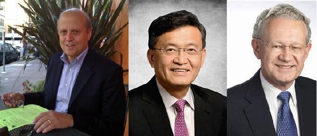
181
2019 Update: EDA
Over the last six years EDA has experienced yet another disruption not
unlike the Synopsys acquisition of Avant! in 2001 which positioned
Synopsys for the EDA lead they still enjoy today. Or the hiring of famed
venture capitalist Lip-Bu Tan in 2009 to be the CEO of struggling EDA
pioneer Cadence Design Systems. Under Lip-Bu's command Cadence has
prospered like no other company in the history of EDA, absolutely.
In 2017 Siemens acquired Mentor Graphics for $4.5 billion representing
a 21% stock premium. Acquisition rumors had been flying around the
fabless semiconductor ecosystem but no one would have guessed it would
be the largest industrial manufacturing company in Europe. At first the
rumors were that Siemens would break-up and sell Mentor keeping only
the groups that were part of Siemens core business, specifically they would
sell the Mentor IC Group. Those rumors were flatly denied at the following
Design Automation Conference during a CEO roundtable and now
182
Mentor, including the IC group, is an integral part of the Siemens corporate
strategy.
While Mentor was the biggest and most disruptive EDA acquisition there
were many others. EDA has always been focused on non-organic growth
(acquisitions) which we track on SemiWiki with our EDA Merger and
Acquisitions Wiki. Synopsys is the largest acquiring EDA company
scooping up EDA and IP companies as well as companies outside of the
semiconductor ecosystem. In the last six years Synopsys has acquired 10
companies involved with software security and quality including the
acquisition of Black Duck Software in 2017 for $547 million. In total
Synopsys has acquired more than 88 companies and we should expect the
acquisition spree to continue.
Mentor financials are no longer public but inside sources say that revenue
growth since the acquisition has by far exceeded expectations based on the
extended reach of the Siemens workforce. Some estimate it to be as high
as 25% growth. Synopsys and Cadence have also prospered since the
Mentor acquisition was announced with revenues and market caps jumping
in a very un-EDA way. Synopsys (SNPS) stock price has almost doubled
and the Cadence (CDNS) stock price has more than doubled. Clearly Wall
Street has a renewed interest in EDA as they should. After all, EDA is
where electronics begins.
Another significant EDA change that has evolved over the previous six
years is the customer mix. Following Apple, systems companies are now
taking control of their silicon destiny and developing their own chips. We
see this on SemiWiki with the domain additions of our expanding
readership. Systems companies now dominate our audience with the rapid
growth of the IP, AI, Automotive, and IoT market segments.
Systems companies are also changing the way EDA tools are purchased.
Rather than buying point tools and assembling custom tool flows (a fabless
tradition), systems companies can buy complete tool flows and IP from
Synopsys, Cadence or Mentor. The "One throat to choke" concept of
183
customer support is a very attractive business strategy for companies
venturing into the world of chip design for the first time.
Systems companies are good candidates for EDA in the cloud which is
finally coming to fruition after many failed attempts. Cadence has been in
the cloud for many years starting with Virtual CAD (VCAD) more than 20
years ago, Hosted Design Solutions (HDS) 10 years ago, and the Cadence
Cloud announcement in 2018 with TSMC, Amazon, Microsoft, and
Google as partners. In 2019 they announced the Cloudburst Platform
which is another important EDA step towards full cloud implementation.
System companies are also not bound by the margin challenges of
traditional fabless semiconductor companies. Apple for example can pay a
much higher price for premium tools and support without notice to their
bottom line. As a result, EDA companies are catering to system companies
by providing and integrating IC tools with system-level design tools. System
based software development is also an EDA target as noted by the recent
Synopsys acquisitions.
EDA has prospered in the last six years like no other time in EDA history
and will continue to do so as semiconductors and electronic products
continue to dominate modern life, absolutely.
185
In Their Own Words: Mentor
Graphics
Mentor Graphics is the oldest EDA company still in
operation. They’ve seen, and helped shape, changes to
technology and business models for over 30 years. In this
section, Mentor shares their history, technology, and their
role in developing the current EDA business environment.
In 1981, Pac-Man was sweeping the nation, the first space shuttle
launched, and a small group of engineers in Oregon started not only a new
company (Mentor Graphics), but also, along with a handful of other
companies, helped launch an entirely new industry, EDA.
Mentor Graphics founders—Tom Bruggere, Gerry Langeler, and Dave
Moffenbeier—left their comfortable, secure jobs at Tektronix, Oregon’s
largest electronics manufacturing company at the time. They were all bright,
ambitious, 30-somethings determined to take advantage of the nascent area
of computer graphics.
They quickly zeroed in on the promising market of computer-aided
engineering (CAE): the automation of schematic capture and simulation
for engineers designing complex electronics systems including printed
circuit boards. The founders spent their first months traveling exhaustively,
interviewing numerous high tech companies about their design challenges. A
preliminary idea for a CAE product started to emerge during this process.
Eventually they decided to focus solely on developing CAE software and
use commercially-available workstations for the hardware.
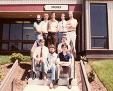
186
Other EDA startups at that time hewed to the time-honored business
model of creating a vertically integrated solution, designing both hardware and
software, stretching precious resources across the two domains.
This decision was risky for many reasons, more so because Mentor’s
founders chose the Apollo workstation as their hardware platform while it
was still only a specification. They personally knew the Apollo founders and
trusted the company could create, on schedule, a new type of computer
that combined the time-sharing capabilities of a mainframe with the
processing power of a dedicated minicomputer. Their calculated gamble
paid off. Creating software from scratch that met specific customer
requirements, while using commercial hardware, proved to be a key
advantage over other fledgling CAE competitors in the early years.
Mentor’s Founders. Clockwise from top left: Charlie Sorgie, Dave
Moffenbeier, Steve Swerling, Tom Bruggere, Jack Bennett. Seated from
left: Gerry Langeler, Rick Samco, Ken Willett, John Stedman.
The Apollo computers were delivered in the fall of 1981 and the Mentor
engineers began developing their software. Their goal was to unveil the first
interactive simulation product, IDEA 1000, at the Design Automation
187
Conference in Las Vegas the following summer. Rather than being lost in
the crowd on the show floor, they rented a hotel suite and invited
participants to private demonstrations. Actually, invitations were slipped
under all the hotel room doors at Caesar’s Palace. Invitations were passed
out indiscriminately to vacationers and conference-goers alike because
Mentor didn’t know which rooms were DAC attendees. The demos were
very well received (by conference goers, anyway).
One of the co-founders, Gerry Langeler, vividly remembers the response
to those first demos:
“I made the presentation while one of our engineers worked the keyboard
of the CAE workstation, and the demonstration software performed
flawlessly. I watched faces go from casual interest to intense scrutiny and
on to slack-jawed disbelief and undisguised enthusiasm. I saw prospects
turn into customers. Word spread. People crowded into the room. People
stood in the hallway craning their necks to catch a glimpse of our
demonstrations. Over the course of the conference, perhaps as many as half
the delegates found their way to our suite. And then came the jackpot: a
purchase order for one system was delivered to us in our suite. We were
bona fide. People had bought the something we had built.”
IDEA 1000 was quickly extended to include a suite of capabilities that
were enthusiastically adopted by engineers creating complex designs for
silicon ICs or printed circuit boards (PCBs). The emergence of these tools
corresponded to the rise of ASIC design. These highly crafted digital ASIC
chips required extensive verification, to ensure correct operation in their
end-system environments. For example, IDEA Station provided complete,
automated schematic capture. Then with Mentor’s QuickSim analysis for
gate-level simulation, designers were able to examine the circuit
functionality before committing to a physical prototype, enabling them to
quickly iterate and improve the quality of the design. IC Station then was
used for the place and route of custom IC designs, reducing the task from
188
weeks or months to just hours. And Board Station performed a similar place
and route functionality for PCB designs.
All three of these products—IDEA Station, IC Station, and Board
Station—became market leading EDA products. Companies across the
electronics industry became major customers, eager to tap the powerful
design, analysis, and implementation capabilities of Mentor’s offering.
Customers included numerous computer companies from Apollo
computer to NEC; semiconductor companies such as Motorola and Texas
Instruments; consumer and telecommunications companies such as
AT&T, Canon and GM/Delco; and large aerospace companies including
Boeing, Rockwell and Lockheed.
With this strong industry response, Mentor became the fastest U.S.
startup company in history to reach $200 million in revenue, reported its
first profit in 1984 and went public the same year. To service all these
customers around the world, Mentor Graphics began opening offices
across the United States, and in Europe and Asia. Throughout the 1980s,
Mentor grew and became one of the most profitable and largest U.S.
startups in the 1980s. Mentor crested the $400 million mark in 1990 and
seemed poised for continued success.
Painful but Healthy Realignments
Unfortunately, all this rapid success for Mentor had an unintended, and
potentially threatening, side effect. The company became a victim of what
has since come to be known as “The Innovator’s Dilemma” (from Clayton
Christensen), listening to their customers’ desire for a single integrated
interface design environment from start to finish. This pursuit of a
“complete solution” flew in the face of what sophisticated customers
clearly wanted—point tools that were best-of-breed which could easily be
integrated into existing flows to meet each emerging design need. This
became increasingly important as EDA startups accelerated their
introduction of innovative design capabilities that needed to be integrated
into a design flow.
189
In addition, the change in the EDA model from bundling software with
hardware changed. Mentor made the tough decision in 1991 to stop
bundling Apollo workstations with the software and to support other
hardware, such as Sun. Mentor revenue peaked at $435 million in 1990 and
then fell as the hardware business disappeared.
Meanwhile, the integrated “framework” under development and now
known as the “Falcon Framework (also called Version 8.0)” proved to be
an overly ambitious undertaking. While Cadence and Mentor pursued
similar approaches, Mentor bet 100% on success of the “framework”
approach and provided no backup for non-framework customers to build
their own environments out of “point tools.” The disruption associated
with development difficulties led to lots of changes, including the
recruiting of a new CEO. Wally Rhines, who was Executive VP in charge
of Texas Instrument’s $5 billion semiconductor business, surprisingly
decided that Mentor offered an opportunity for innovation and growth,
heralding the beginning of a new direction away from the “framework”
approach.
Back on Track
Rhines came to Mentor with an extensive understanding of the electronic
design process, having managed most types of semiconductor businesses,
as well as a $1 billion minicomputer and computer peripherals business.
His success at TI had been propelled by the success of digital signal
processing where he first supervised the development of a chipset used in
“Speak ‘n Spell,” a talking educational product, and then the conception,
development and commercialization of a complete family of digital signal
processors, the TMS 320 family, which eventually evolved to become
nearly half of TI’s total revenue.
Rhines spent his initial time at Mentor stemming the bleeding from
Version 8.0 and redirecting the company to a strategy that could easily
accommodate non-framework based point tool developments, both by
Mentor and by third parties, into useful design solutions. One month after
190
his arrival, Mentor acquired Checklogic, which eventually evolved to the
industry’s leading design-for-rest solution and stimulated two of the most
significant discontinuities in DFT—compression and cell-aware test. Three
months after his arrival, a major initiative to develop a new generation of
physical design verification was kicked off, since Mentor’s Checkmate
product, which had achieved only moderate success against Cadence
Dracula, had been licensed from Wally himself when he was at TI (after
Cadence acquired ECAD which provided the Mentor Dracula OEM
product), and Mentor had the capability to develop its own unique
approach to physical verification.
These needs quickly evolved into a new strategy for Mentor, completely
different from the “own the whole flow” strategy of Version 8.0:
1) Focus where you can be #1, but support open standards so that you
can be easily integrated into all design flows
2) Look for design discontinuities to replace existing solutions
3) Identify new emerging problems and develop the tools that will be
needed before the problems become big issues
While Mentor had lost time, momentum, and its #1 market share
position to the Version 8.0 diversion, the company quickly began making up
for lost time. Having led the EDA industry in gate-level simulation with
Quicksim, Mentor developed an early RTL simulator for the newly emerging
multi-company VHDL standard which was supported by much of the
customer base as a counter to Verilog which was developed as a proprietary
simulator. With the acquisition of Model Technology, Mentor was able to
provide the industry’s first direct-compile simulator which, because of its
“single kernel,” quickly supported VHDL, Verilog and subsequently System
Verilog, C++, System C and other languages. Mentor was therefore able to
sustain its #2 market share position in RTL simulation for the next 18 years
(except for the years that it became #1, according to GSEDA).
191
Meanwhile, the Calibre product team of three core people, Laurence
Grodd, Koby Kresh, and Robert Todd, built upon their long experience
supporting Dracula and Checkmate to develop a totally new approach to
physical verification using “hierarchy” as a way to dramatically impact
performance. Operating as a virtual “skunkworks” in Mentor Graphics, the
team worked with customers that were outside the targeted IC Station user
base, running benchmarks without Mentor management awareness. By late
1996, word got out that Mentor had something really unique and the
adoption of Calibre took off as users of existing physical verification
software found that they couldn’t verify large designs at 250 nm and below.
A long series of innovations followed over the next several years, leading to
a total of 48 patents granted to the Calibre core team and eventually Calibre
expanded into a full platform for physical verification, analysis and design-
for-manufacturing. The team made sure that Calibre was so well integrated
with competing design flows that compatibility hardly ever became an issue.
Other Changes in Leadership and Direction
In 1996, Mentor recruited Greg Hinckley, former Senior VP and CFO of
VLSI Technologies to become COO (and CFO) at Mentor. Greg’s “out of
the box” thinking, analytical skills, and business experience made him and
Rhines close partners in the management of Mentor and accelerated the
focus on innovation. From his experience at VLSI, Greg attracted Don
Maulsby to manage Mentor Worldwide Sales and Henry Potts to run the
PCB business. While most companies believed that PCB was a “dead”
EDA business, Greg and Wally combined their contrarian views and placed
new emphasis on emerging opportunities in system design. Building upon
a #1 market share position in PCB, Henry Potts expanded the system
design business into totally new areas like signal integrity, thermal analysis
and, most importantly, transportation system design. Complemented by
Serge Leef ’s interest and developments in automotive network analysis and
an emerging new standard called AUTOSAR, the systems design activity
thrived and became the fastest growing major business during the 2000s.
192
To complement hardware design, Mentor entered the embedded
software business via the acquisition of Microtec (the largest embedded
software company and owner of the VRTX RTOS) in 1996 and later
companies like Accelerated Technologies (owner of the most widely used
RTOS, by number, NUCLEUS).
By this point, Mentor’s strategy of building upon its #1 market share
positions, like PCB, and identifying technical discontinuities in existing
flows such as Calibre, was producing results and the revenue in the late
1990s and beyond grew somewhat faster than the overall industry. But it
was the identification and support for newly emerging design problems—
the third leg of the strategy—that fueled the next wave of growth. These
included:
• The emergence of the need for emulation for both hardware
and software verification
• Adoption of embedded software development environments by
chip and system development teams
• Application of the basic tools of electronic design automation to
system design, particularly for planes, trains, cars, and distributed
networks
• High-level ESL design
• Resolution enhancement for design for manufacturing (DFM)
• Adoption of open source software and LINUX-based
embedded development environments
• Enhancements to existing capabilities such as: Compression and
cell-aware ATPG; Push-button formal methods for simulation;
Intelligent test benches; High-level power analysis, and many more
193
One of the most exciting developments was the invention of compressed
test by Janusz Rajski. The automatic test equipment industry (ATE) had
been unable to keep test cost in line with the overall manufacturing cost
per transistor, making test a rapidly increasing portion of the total cost of
manufacturing. Janusz developed a technology that would initially allow
first for 10X compression of test patterns, and a similar reduction in test
time, and then improved it to more than 200X on average, with a clear
roadmap to 1000X. This was a major factor in Mentor becoming the #1
provider of EDA test solutions. More recently, development of Cell-Aware
ATPG is proving to be a similar game changer, offering order of magnitude
improvement in test quality as well as the unique ability to reliably test parts
that contain FinFETs.
Open Standards Pave the Way
A key enabler contributed to Mentor’s role as the only #1 EDA
company to fall from grace and then recover to become a top contender
once again. That was the role of standards. Because of the failure of Version
8.0, Mentor became an aggressive supporter of open standards to integrate
tools and platforms into flows, especially flows dominated by competitors.
Mentor made this part of the accepted culture, giving as well as receiving.
Whenever a Mentor approach became popular, it became a candidate to
donate to a standards organization. Among the list of contributions that
were wholly, or partly, from Mentor are: UPF,
SystemC, UCIS, OASIS, JEDEC, IJTAG, VHDL, OpenDFM, and
OpenPDK among others. This preoccupation with standards led to
interesting competitive situations.
For example, TI, Nokia, and Mentor developed a standard for power
management that Mentor implemented in its simulators about year 2000.
As other customers found a need for it, Mentor enlisted Synopsys and
Magma to join Mentor in an Accellera-sponsored standardization.
Similarly, when Mentor’s Advanced Verification Methodology (AVM)
approach to simulation gained popularity versus a proprietary approach
194
called Verification Methodology Manual (VMM), Mentor and Cadence
joined forces to provide a design methodology called Open Verification
Methodology (OVM). A widely-accepted standard was born and became
the basis for what is now called Universal Verification Methodology
(UVM). One of the most interesting was the early adoption of System
Verilog. Synopsys solicited Mentor’s participation, believing that Mentor
would be relatively passive. When Mentor became first to market with
System Verilog by more than a year, the industry changed and so did
Mentor.
Litigation Strikes
Mentor avoided litigation wherever possible, but sometimes it just wasn’t
possible. One case occurred in 1997. Mentor was an early pioneer in the
technology of hardware acceleration, or emulation, introducing a key
product in 1988. Subsequently, Mentor sold this technology to a startup
called Quickturn. This proved to be an expensive mistake. Rhines, who had
been a big fan of emulation since his integrated design experience starting
in the mid-1970s, initiated emulation development as soon as he arrived at
Mentor. As Mentor became successful, it had to defend itself against its
own patents that had been sold to Quickturn (now Cadence). Subsequently,
departure of the emulation design team led to other patent litigation, all of
which detracted from more productive uses of time. But the story has a
happy ending, as Mentor’s engineering team developed the industry-leading
Veloce hardware acceleration platform and reclaimed the number one
position in emulation in 2013.
System Design Focus
Because EDA in the early 1980s included both chip and board design,
Mentor won the race very early for the hearts and minds of the automotive
and military/aerospace customers. These customers developed stable,
broad infrastructures for designs that didn’t change quickly. Recognizing
that strength, Mentor paid a lot of attention to these customers and actually
195
invested a higher percentage of R&D in the last 15 years in system design
than in EDA as a whole. The result was a firm foundation when these
system companies began automating their design processes in the same way
that semiconductor companies had done several decades before.
For Mentor, this included tools to automate the virtual design of cars, trains,
planes, and bigger systems. Introduction of design tools for automotive
interconnect design in 1992 evolved to a major thrust under Martin O’Brien
in year 2000 and the evolution of the Capital family of enterprise design
tools, from architectural concept through electrical design/analysis, cost
tradeoff analysis, manufacturing set-up/bill of materials, and service and
support. This was complemented by families of automotive design
products developed by Serge Leef ’s group that included network analysis
and the industry’s first AUTOSAR design tools to support an emerging
automotive design standard. The addition of an open source software team
under Mark Mitchell and an embedded software development capability
under Scot Morrison provided Mentor with unique capabilities for a rapidly
growing transportation market.
Today, the application of EDA to systems design is driving growth that is
substantially greater than the growth of adoption of traditional chip design
automation.
Innovations in Higher Levels of Abstraction
Mentor was a very early investor in the emerging Electronic System Level
design abstraction, referred to as ESL. For about 15 years, Mentor was the
only major EDA company with substantial revenue in this product space.
Development of Seamless, the EDA industry’s first successful
hardware/software co-verification product, was an early achievement, as
was Catapult C, a high-level synthesis product. But it was evident that a
more complete solution to the high-level design challenge was needed. One
of Mentor’s competitors began bidding a high price for Calypto, a company
that had developed high-level power analysis and optimization tools and it
was clear that an integrated flow with Calypto would have value for
196
customers. Because Mentor couldn’t offer such a high price, it proposed an
in-kind approach, spinning off the Catapult business into a combined entity
with Calypto and retaining ownership in proportion to the revenue and
profit contribution. The combined company flourished and operated
independently of Mentor. Meanwhile, Mentor retained Vista, a high-level
design product developed by its Israeli team under Guy Moshe, and found
itself early in the race to high-level power/ performance analysis.
Doing What Others Don’t Do
With the arrival of Greg Hinckley at Mentor, Wally had reinforcement
for his natural contrarian inclinations and Mentor increasingly explored
areas outside the traditional space of EDA. One of the early efforts involved
embedded software, beginning with the acquisition of Microtec in 1996 but
continuing with increasing emphasis as embedded software became a more
important part of every electronic design team. Thermal analysis and
computational fluid dynamics was another area that attracted Mentor
interest, becoming more than 5% of revenue in 2013. And Mentor fearlessly
entered totally new areas like hardware for analysis of thermal inertia and
for designing lighting systems. The continuing emphasis on systems design
opens the door to dozens of new possibilities in the future.
Single-Vendor Flows
While Mentor championed best-in-class tools and the capability to
smoothly integrate tools from third parties into Mentor flows, there was at
least one case of customer support for a single-vendor approach. This was
in the area of printed circuit board design and manufacturing. As PCB
design matured, and Mentor’s market share approached 50%, many
customers began pushing for a flow that would integrate everything from
concept through manufacturing deployment and yield improvement. The
acquisition of Valor in 2010 completed that flow and led to a variety of new
capabilities.
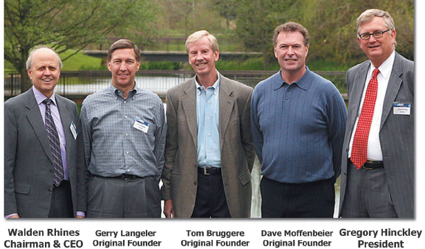
197
Mentor’s founders with the current company leaders in
2001 during Mentor’s 20
th
-anniversary celebration.
Photo courtesy of the Wilsonville Spokesman.
Calibre Goes Beyond Verification
As Calibre became a de facto standard for physical verification, more and
more capabilities were added. Design-for-manufacturing became a big issue
and a wide variety of tools for modeling lithography hot spots and yield
limitations were required. Optical proximity correction continued to evolve
to new levels of sophistication.
But one of the most interesting was the evolution of yield enhancement
capabilities. A number of customers suggested that because Mentor was
the leader in both design-for-test and physical verification, we should
consider combining the two databases to look for systematic layout
problems. That is, take the massive volume of test data and correlate it with
physical layouts to look for “outliers” that showed statistically anomalous
failure rates. The family of yield enhancement products introduced in 2005
grew to be a cornerstone of yield enhancement (and profit improvement)
for the semiconductor manufacturing industry.
198
The Future
What makes the outlook so bright for Mentor Graphics? After all, the
semiconductor industry is only growing at a 5-7% rate and the EDA
industry has traditionally grown at the same rate as semiconductor R&D,
being limited to about 2% of total semiconductor revenue.
There are two basic phenomena that provide for excitement and future
growth. First, the semiconductor industry technology regularly adopts new
technologies, each of which leads to a spurt of growth for the newly needed
EDA tools. Recent examples of this have been:
• The need for reliability analysis tools for electrostatic discharge and
electromigration analysis that made Calibre PERC a de facto approach.
• Evolution of 3D IC production that required a new set of verification
tools (Calibre 3D) and a new approach to design-for-test with the
Tessent suite of products.
• New requirements for quality that led to the development of Cell-Aware
ATPG to detect transistor-level defects with gate level test patterns,
and many more.
The second phenomenon is the inevitable adoption of EDA technology by
the systems industry. To a first approximation, the systems industry uses
EDA at about the same level as the semiconductor industry did in the
1960s. Building and testing physical prototypes has been the standard way
that industries begin their path to design automation. Electronics sold with
systems like cars, planes, and industrial equipment total around two trillion
dollars per year, compared to the $300 billion of semiconductor electronics
sold each year. As the systems industries adopt EDA, it’s likely that they too
will spend a percentage of their revenue in the quest for automation,
making today’s EDA revenue seem trivial by comparison. Mentor’s early
history in system design, as well as its survival as the oldest major EDA
company, provides the basis for leading this next revolution.
199
What’s Next in EDA?
The history of EDA industry growth has been driven by the emergence
of new design challenges. The early generation of schematic capture and
simulation was quickly augmented by PCB design, IC place and route, and
physical verification. In the last ten years, virtually all EDA industry growth
has come from totally new design methodology requirements, e.g. sale of
IP blocks, resolution enhancement, ESL, formal verification, design for
manufacturing, and a few more. The best assumption is that the future will
evolve as it has in the past, i.e. solutions to new design problems as well as
the application of EDA technology to challenges in other areas of design.
With the evolution of IC design into the 14, 10 and 7 nm realms, there
will be requirements for analysis of new physical design problems.
Examples include reliability, electromigration, thermal effects, stress, EUV
resolution enhancement, and yield analysis. Even larger will be the adoption
of electronic design automation by system design companies that have been
able to get by with semi-manual methods in the past. Automotive and
aerospace applications are the most obvious since the electronic complexity
of cars and aircraft is increasing so rapidly, probably 5% per year or more.
How long will it be before we simulate the electronic behavior of an entire
car or plane? A long time. But the capability to design and optimize the
electrical interconnect, verify correct operation of safety, environmental
and security features, manage the tradeoffs in cost and weight versus
performance and provide a complete electronic database that can be used
by automotive engineering, manufacturing and service is already here and
will be a big part of EDA industry growth in the next ten years.
201
2019 Update: Mentor Graphics
A New Era for EDA and Mentor
Looking over the past decades of Mentor’s and EDA’s combined history,
it is apparent that major inflection points have occurred to address
emerging design challenges. EDA 1.0 enabled the Gate Level Era, where
designers relied on electronic schematic capture and custom place and
route tools to move beyond the tedious and limitations of hand layout.
EDA 2.0 ushered in the RTL Era that made ASIC design possible with the
advent of RTL synthesis, automated place and route and advanced
photolithography capabilities. About a decade ago, EDA 3.0 unleashed the
Blocked-Based Era relying on new design methodologies such as resolution
enhancement, formal verification and design for manufacturing to create
enormously complex SoC with billions of transistors.
Now we are moving into a new era, EDA 4.O IC to Systems Era focused
on the role the ASIC plays in an unprecedented number of smart systems.
As an EDA company, Mentor has always been unique in the industry for
having a sustained focus on both IC as well as system design: whether it is
PCB design, embedded software for ICs, multiphysics system analysis,
system emulation or electrical systems, networks and harnesses. That is why
Mentor has long held a vision of the future where the IC is part of a bigger
system and, ultimately, the end product.
Anticipating the advent of EDA 4.0, Mentor Graphics and Siemens
announced in November 2016 they had entered into a merger agreement.
202
The addition of Mentor decisively extends Siemens' Digital Enterprise
Software portfolio with Mentor’s well-established electronics IC and
systems design, simulation and manufacturing solutions. Mentor is now
part of Siemens’ software business, making the combined organization the
world’s leading supplier of industrial software for system design,
simulation, verification, testing and manufacturing.
The partnership with Siemens provides increased resources, customer
relationships and new technologies. We are now a valued contributor
within a global fortune 100 company that believes in a future of increasing
virtual design of electronics and of systems. Siemens’ strong foundation in
data management, mechanical CAD, device modeling, computational fluid
dynamics, and other technologies provides a wealth of resources for
Mentor to accelerate our customers’ design competency.
These capabilities are essential for EDA 4.0 smart, connected products—
from smartphones and household appliances, to automobiles, aircraft and
machinery and autonomous vehicles. At the heart of the systems is the IC,
providing the intelligence for these smart products. Under the guidance of
Joe Sawicki, executive vice president of Mentor IC EDA, we will continue
to invest in developing world-class capabilities for IC design, verification
and test.
Beyond the IC, the combined strengths of Mentor and Siemens provides
mechanical, thermal, electronic and embedded software tools that
customers can deploy to further accelerate their innovation, drive
production efficiencies and optimize the operation of their products in the
field. Now, for the first time, quality, efficiency, flexibility, safety and speed
can be optimized across technical domains, throughout the entire lifecycle
of a system and for the entire extended enterprise.
For example, automotive design has traditionally been driven by
mechanical design. Now the differentiation and capability of cars is
increasingly IC-based electronics. That’s why total system simulation has
become a requirement. The basic task of “sensor fusion”—as more and
203
more electronic sensors for visual, radar, and lidar are attached to the car—
has stimulated new electronic architectures. There is no way to reliably
design vehicles and aircraft without virtual simulation of electrical
behavior. Beyond the automotive and aerospace markets, there are a host
of new system technologies that require new electronic and IC
capabilities—the Internet of things, artificial intelligence and machine
learning, to name a few.
The Siemens’ era has been marked by increases in collaboration with
traditional EDA rivals, notably Synopsys In July 2018 Synopsys and
Siemens PLM settled a long-running emulation patent dispute (originally
between Synopsys and Mentor). The settlement included not only a seven-
year patent cross-licensing agreement but also a slew of collaboration on
EDA design and verification interoperability projects between the two
companies.
With Siemens, Mentor now has the resources to expand into new areas,
especially the interface between system and IC design. Committed to
accelerating Mentor’s growth, Siemens is investing aggressively in Mentor’s
R&D, both in integrated circuit design and system EDA— ranging from
5G and analog designs to machine learning and ISO 26262 verification.
Several key acquisitions attest to this commitment.
• Austemper Design Systems strengthens Mentor integrated circuit
(IC) design and verification technology for automotive by enhancing
ISO 26262 functional safety testing via Siemens’ digital twin offering.
• Sarokal Test Systems adds to Mentor’s growing IC strength and
worldwide digitalization strategy with unique technology and
expertise for the 5G communications segment.
• COMSA’s LDorado addresses the demands of electric and
autonomous vehicle development with key capabilities in wire
harness engineering and design data analytics.
204
• Solido Design Automation makes Mentor the leading provider of
variation-aware design and characterization software.
Ready for the Challenges of the Future
EDA will enable tomorrow’s smart systems to drive intelligence to the
edge in every conceivable industry and market. Already smart technologies
are being developed deployed in cities, factories, homes and the office. At
the same time, intelligent systems are revolutionizing energy (smart grid),
transportation (autonomous drive) and moving goods (smart supply chain).
Joe Sawicki, EVP of Mentor IC EDA sums it up: “All of this is spurring
ever more sophisticated IC design based on artificial intelligence and
machine learning. EDA 4.0 provides the IC innovation and system design
expertise to enable this new era of low-cost, low power intelligence at the
edge.”
Mentor with Siemens is eager to be a part of helping design for this
exciting future. Indeed, EDA 4.0 seems poised to be a key enabler of the
Industry 4.0 industrial transformation underway, led and championed by
Siemens at the highest levels of the company.
205
In Their Own Words: Cadence
Design Systems
Cadence Design Systems has been a key player in the
semiconductor and electronics ecosystem for a quarter century.
In this section, Cadence shares its history, technology, and its
role in developing the EDA business environment.
Cadence is a leading EDA supplier with comprehensive solutions for
custom/analog IC design, digital IC design, functional verification, and IC
packaging and printed circuit board (PCB) design. In addition to these
“traditional” EDA domains, Cadence is also developing new solutions for
system-level design and verification and is adding to a growing portfolio of
design IP and verification IP. Cadence today has deep partnerships with
customers, foundries, and IP providers.
In 2013, Cadence® celebrated its 25th anniversary. That’s because two
mid-sized EDA vendors—SDA Systems and ECAD—merged in 1988 to
form Cadence. However, the Cadence story goes back well before 1988, to
the founding of ECAD and SDA Systems in 1982 and 1983, respectively.
ECAD was founded by Glen Antle and Paul Huang. Both were working
at the Systems Engineering Lab (SEL) when the CAD group developed a
new, and very fast, algorithm for design rule checking (DRC). Huang
directed the development of this IC physical verification technology. In
1982, Gould Inc. bought SEL, and Gould granted Antle and Huang the
marketing rights to the technology.
206
Antle and Huang launched ECAD, and the DRC software became
Dracula, one of the EDA industry’s best-known products in the 1980s and
1990s. ECAD also developed Symbad, an IC layout product line.
ECAD was an unusual EDA company in the 1980s because it sold only
software that supported workstations and computers from multiple
providers. In the early 1980s, the “big three” EDA companies (then called
computer-aided engineering, or “CAE”) were Daisy Systems, Mentor
Graphics, and Valid Logic. All derived a considerable share of their
revenues from selling workstation hardware. But ECAD was nonetheless
consistently profitable, and it went public in 1987.
SDA Systems, like so many other good things in Silicon Valley, started
with a dissatisfied engineer. And not just any engineer—Jim Solomon, SDA
founder, was a renowned analog engineer with a string of accomplishments
at Motorola and subsequently at National Semiconductor. Solomon was
frustrated by the lack of analog CAD tools, and he saw the need for a
standard format for design data storage.
Solomon wrote a business plan while at National Semiconductor, and
while he didn’t originally intend to run a new company, that’s what
happened. SDA received start-up funding from National Semiconductor,
General Electric, Harris Corp., and L.M. Ericsson. The company
developed an integrated suite of IC physical design tools. Perhaps SDA’s
biggest contribution was the idea of a “design framework,” developed in
co-operation with the University of California at Berkeley professors
Richard Newton and Alberto Sangiovanni-Vincentelli. The SDA
framework provided a common user interface and database, and allowed
engineers to integrate tools from a variety of sources.
In 1984, Joe Costello, who would later become the first CEO of Cadence,
left National Semiconductor to join SDA Systems as vice president of
customer service. In 1987 he became SDA Systems president and chief
operating officer. Like ECAD, SDA was a successful software-only EDA
207
company. In September 1987 SDA filed for an IPO, but the October stock
market crash derailed those plans.
As the EDA market rapidly expanded in the 1980s, ECAD and SDA
realized they could best take advantage of new opportunities by teaming
up. In February 1988, ECAD agreed to acquire SDA in a stock swap valued
at $72 million. The merger was completed May 31, 1988, and the company
was incorporated June 1
st
as Cadence Design Systems. Huang became a
vice president of R&D, Solomon became president of the Cadence Analog
Division, and Costello was named Cadence president and CEO.
1989—A Quick Start Out the Gate
1989 was a formative year for the young company in several respects.
Cadence completed two strategic acquisitions, launched the Analog
Division, and experienced rapid growth, quickly becoming the leading
provider of IC CAD tools. Like ECAD and SDA, Cadence continued a
“software-only” EDA model, supporting popular third-party workstations and
computers.
In March 1989, Cadence acquired Tangent Systems, a provider of timing-
driven placement and routing software. The acquisition propelled Cadence
to the #1 spot in IC CAD. Tangent’s Tangate product became Cadence
Gate Ensemble, and Cadence Cell3 Ensemble was an adaptation of Gate
Ensemble for standard cell-based design. These products took leadership
positions in ASIC placement and routing, and they became a major revenue
source for Cadence.
In November 1989, Cadence acquired Gateway Design Automation,
developer of the Verilog language and Verilog-XL simulation software. The
Verilog hardware description language (HDL) represented a new way to do
chip and systems design. Instead of drawing gates on a schematic, designers
could write code at the register-transfer level (RTL), greatly amplifying
productivity.

208
In the late 1980s, most other EDA vendors were promoting VHDL, an
HDL that had Department of Defense (DoD) backing. But Verilog users,
already familiar with the C-like language, remained fiercely loyal. Cadence
offered Verilog as an open standard, and today Verilog and its
SystemVerilog cousin—both IEEE standards—are far more widely used
than VHDL.
Starting with technology initially developed at Harris Semiconductor, the
Cadence Analog Division produced Analog Artist, a full-custom IC design
software environment that provided schematics and simulation and included
a layout editor. A Lisp-based language called SKILL® provided user
programmability of the toolset.
Cadence CEO Joe Costello speaks at the Design Automation
Conference in 1997. (Photo courtesy of Design Automation
Conference)
Analog Artist set the stage for continuing Cadence strength in the analog
IC CAD market. After many years of improvements, Analog Artist evolved
into the current Cadence Virtuoso® Analog Design Environment (ADE).
SKILL is still widely used to develop process design kits (PDKs), generate
parameterized cells (PCells), and interact with and customize tools,
including Virtuoso custom/analog IC tools and Cadence Allegro® PCB
209
design tools. Under Costello’s charismatic leadership, Cadence grew rapidly
during this period. The number of employees went from 433 in 1988 to
978 in 1989. According to Dataquest, Cadence held 44.2% of the $172.3
million IC CAD market in 1989. In 1990, Cadence became the second
largest EDA provider, following Mentor Graphics.
Cadence in the 1990s—New Technology and Rapid
Expansion
Cadence grew quickly in the 1990s. The growth was fueled by both
internal R&D development and a number of strategic acquisitions. In 1991,
Cadence acquired Valid Logic, which was then the third-largest EDA
vendor in terms of revenues. As a result of this acquisition, Cadence became
the EDA revenue leader, a position held for much of the next two decades.
While Cadence was already strong in IC design, Valid’s area of strength was
system design, which involved multi-chip systems and boards. Here are
some other key developments that took place in the 1990s:
Continued Development of Analog/Mixed-Signal Offerings
In 1991, Cadence launched the Spectre® simulator, which is still a key
offering. This circuit simulator could handle larger circuits than SPICE and
run up to 10 times faster. Also in 1991, Cadence brought out the Analog
Artist Layout Editor, which linked layout with schematics. Incremental
improvements to Cadence analog/mixed-signal products continued
throughout the decade, and the Virtuoso name came to identify the Cadence
family of custom/analog tools.
Pioneering Work in System-Level Design
System-level design is still thought of as a “new” area in EDA although
it’s been around for a long time. In the 1990s, Cadence was a pioneer of
this technology, then called electronic system design automation (ESDA).
In 1993, Cadence acquired Comdisco Systems, which provided a graphical
DSP design tool called Signal Processing Workstation (SPW) and a network
210
analysis tool called Block-Oriented Network Simulator (BoNES). Cadence
then formed the Alta Group to focus on ESDA.
In 1994, Cadence moved further into ESDA by acquiring Redwood
Design Automation, which had developed a system-level simulator. In
1998, the existing Alta products were merged into the Cadence mainstream,
and the Felix Initiative was launched to develop an ambitious new level of
ESDA tools.
A more immediate step up in abstraction, however, was taking place as
engineers made the move from gate-level schematics to RTL design using
VHDL or Verilog. Logic synthesis from RTL code to a gate-level netlist
was an important part of this methodology. In 1994 Cadence offered a suite
of “placement-based” synthesis tools. To bolster its synthesis offerings,
Cadence acquired a synthesis startup, Ambit Design Systems, in 1998.
Continuing Innovation in Placement, Routing, and Physical
Verification
IC placement and routing and IC physical verification were major
Cadence strongholds throughout the 1990s. Cadence continued to
innovate in IC physical design in response to rising chip complexity and
the move to “deep submicron” designs (meaning process nodes below 1
µm).
Developed at ECAD, the Dracula physical verification product helped
Cadence cement its early lead in IC physical design. But in the mid-1990s,
Dracula was running out of steam for large designs. In 1995, Cadence
introduced Vampire, a hierarchical successor to Dracula that ran 2X to
100X faster.
In 1996, Cadence rolled out Silicon Ensemble for IC placement and
routing. In 1999, Cadence brought out Silicon Ensemble Ultra, a next-
generation IC physical design solution for 0.18 µm designs.
211
Bringing Peace to the “Language Wars”
Cadence placed the Verilog language in the public domain in 1990 and a
new organization, Open Verilog International (OVI), was chartered to take
responsibility for the nascent standard. Cadence continued to provide
Verilog simulation tools. Most other EDA vendors, however, were strongly
supporting VHDL, and a “language war” between Verilog and VHDL
began. Over time, many loyal Verilog users resisted the move to VHDL,
and other EDA companies began to provide tool support for Verilog.
In May 1992, Costello gave a keynote speech at the VHDL International
(VI) User’s Group. He called for an end to the “HDL wars,” called on OVI
and VI to work together (they later merged to form the Accellera standards
organization), and said that Cadence was 100% committed to supporting
both languages. In the early 1990s, Cadence offered a VHDL-XL simulator
(in addition to Verilog-XL) and then rolled out a new VHDL simulator
called Leapfrog.
Cadence entered the formal equivalence checking market with Affirma
in 1998. Also that year, Cadence acquired Quickturn Design Systems,
gaining the technology that became today’s highly successful Palladium®
platforms for simulation acceleration and emulation.
Corporate News—A Civil and Criminal IP Rights Case Stuns
Silicon Valley
In the early 1990s, an IC placement and routing startup called ArcSys,
later re-named Avant!, was challenging established EDA vendors including
Cadence. But Cadence executives began to suspect misappropriation of
Cadence source code. In December 1995, a police raid on Avant!
headquarters in Sunnyvale, California seized potential evidence and kicked off
a five-year legal battle among the county, Avant!, and Cadence.
Cadence filed suit against Avant! over the alleged theft of Cadence source
code. Avant! countersued, and the two companies went to court many
times over the next five years. Eventually, criminal charges were filed
212
against Avant! and several executives as well. At the conclusion of this legal
drama in 2001, Avant!’s chairman and six other individuals pleaded no
contest to the criminal charges. Avant! was ordered to pay restitution to
Cadence.
Finally, in late 2001, Synopsys purchased Avant! for $780 million—at the
time, the largest acquisition in EDA history.
In other corporate news, Cadence acquired PCB routing pioneer Cooper
& Chyan Technologies (CCT) in 1996. This not only brought Cadence new
routing software, but also a new CEO. In 1997, Jack Harding became
Cadence’s CEO after serving as CEO at CCT. Harding was succeeded as
CEO at Cadence in 1999 by Ray Bingham, who had previously been
Cadence’s CFO.
Cadence in the 2000s—Strengthening Technology, Driving
Standards
In the 1990s, Cadence built a solid foundation covering almost every
aspect of EDA—including custom/analog design, digital IC design,
functional verification, PCB design, and system-level design. In the 2000s
Cadence built upon that foundation, and brought forward new technology
both from internal R&D and external acquisitions. Cadence also played a
key role in EDA standards development, especially with the OpenAccess
database, Common Power Format (CPF), and Universal Verification
Methodology (UVM).
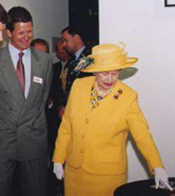
213
A Standard Data Model for the EDA Industry
While there have been many EDA standards efforts, OpenAccess may
be the most successful and impactful of all. Today, the OpenAccess
standard and the reference implementation are widely used by EDA
vendors, fabless semiconductor companies, IDMs, and foundries. Cadence
continues to maintain and upgrade the reference implementation as a
service, at no cost to the industry.
Cadence CEO Ray Bingham (center) meets Queen
Elizabeth II in 2000 at the Cadence Livingston
Design Center in Livingston, Scotland.
The OpenAccess effort began in the 1990s, when large EDA
customers—including some who were just starting to buy commercial
tools—decided they wanted a common data model and C++ API to
provide interoperability among EDA tools. The user companies coalesced
into the OpenAccess Coalition under the Silicon Integration Initiative (Si2).
When Si2 put forth a request for technology in 2001, Cadence responded
by contributing what was then called its Genesis database.
Currently the Si2 OpenAccess Coalition still manages the standard,
allowing companies to download the OpenAccess data model, API, and
reference database.
214
Acquisitions Provide Capabilities for Leading-Edge IC Designs
A spate of acquisitions in the 2000s helped Cadence integrate the latest
and greatest technology into its IC design tools. They included the
following:
• 2001: Purchase of CadMOS brought tools for noise analysis, physical
verification, and signal integrity, including the CeltIC® cell-level noise
analysis tool. Charlie Huang, present-day senior vice president for
Worldwide Field Operations and the System & Verification Group at
Cadence, was CadMOS co-founder and CEO.
• 2001: Acquisition of Silicon Perspective included the First
Encounter® silicon virtual prototyping tool.
• 2002: Cadence bought Plato, developer of the NanoRoute® system-
on-chip (SoC) router that’s still in use. NanoRoute technology was
integrated into the Cadence SoC Encounter™ product, the
forerunner of the present-day Encounter Digital Implementation
System.
• 2002: The Simplex Systems acquisition provided advanced technology in
3D parasitic extraction, power grid planning, electromigration, and signal
integrity analysis, as well as a highly-respected design services group.
• 2003: Purchase of Get2Chip synthesis startup brought new RTL
synthesis technology that formed the basis of today’s RTL Compiler.
Get2Chip had also developed physical synthesis (integration with
placement) technology. Chi-Ping Hsu, Chief of Staff at Cadence, was
president and CEO of Get2Chip.
• 2006: Design for manufacturability (DFM) was a big issue at this time,
as designers began working at 90 nm and below. Cadence purchased
Praesagus in 2006 and Clear Shape in 2007. Both of these DFM
215
companies focused on the impact of manufacturing variability.
Invarium, acquired in 2007, provided lithography modeling.
• 2008: Cadence acquired Chip Estimate, provider of chip planning
tools and the ChipEstimate.com™ silicon IP portal, which is still
heavily trafficked.
Metric-Driven Approach Redefines Functional Verification
In the 2000s, functional verification emerged as a major bottleneck in the
IC design cycle. With advanced process nodes, it became possible to place
tens of millions of gates on a single chip. Conventional approaches to
simulation broke down, and a paradigm shift was needed. Such a shift came
about through the Cadence purchase of Verisity in 2005, which brought to
a larger marketplace new ideas such as reusable verification methodologies,
constrained-random testbench generation, metric-driven verification with
functional and code coverage, and use of verification IP (VIP).
Before the acquisition, Verisity was a relatively young EDA company
focused exclusively on verification. They had a dedicated verification
language, called “e”, which is still widely used and was even adopted as an
IEEE standard (IEEE 1647). Verisity developed the eRM (e Reuse
Methodology), which later provided a foundation for the Open Verification
Methodology (OVM) offered by Cadence and Mentor Graphics. OVM, in
turn, was the basis for today’s Universal Verification Methodology (UVM),
which is now supported by all major EDA vendors.
Verisity also provided the Specman® verification environment, which
included such features as automatic test generation, data checking, and
functional coverage analysis. Verisity pioneered “coverage-driven
verification,” an approach in which engineers run simulation, collect
coverage metrics, and use the metrics to determine whether additional
testing is needed. Cadence integrated Specman technology into the
Cadence Incisive® verification suite, and refined coverage-driven
verification into what is now called “metric-driven verification.” In the
216
2000s, Cadence also moved forward in formal verification. The 2003
purchase of Verplex Systems brought Cadence the widely-used
Conformal® product line. In 2005, Cadence released Incisive Formal
Verifier, which helps designers verify assertions in RTL code.
A New Way to Describe Power Intent
Low-power IC design emerged as a big concern in the 2000s. Engineers
started using low-power design techniques such as clock gating, multiple
threshold voltages, power shutoff, and voltage islands. But there was no
standard way to specify power intent.
In 2006, Cadence launched the Power Forward Initiative along with
Applied Materials, ARM, AMD, Fujitsu, Freescale, NEC, NXP, and TSMC.
The organization was chartered to develop the Common Power Format
(CPF), which could describe power intent for multiple tools in a single file.
In December 2006, Cadence contributed the CPF format to Si2 and in
March 2007, the first version of the CPF standard was available to everyone
in the industry. It has been successfully used in hundreds of SoC designs.
Cadence competitors led an effort to develop another power format, the
Unified Power Format (UPF), which started in Accellera and is now the
IEEE 1801 standard. Cadence is actively involved in IEEE 1801 Working
Group and is working with customers and other suppliers toward
convergence between the two formats.
Continued Improvements in Custom/Analog Design
In the 2000s, Cadence continued to improve its core strength in
custom/analog IC design. In 2004, the company acquired NeoLinear,
which developed a circuit sizing tool. Tom Beckley, present-day senior vice
president for the Custom IC & PCB Group at Cadence, was president and
CEO of NeoLinear.
In 2006, Cadence re-tuned the Virtuoso environment to offer a
constraint-driven flow and run on the OpenAccess database. This opened
217
the door to the present-day Cadence mixed-signal capability, which uses
OpenAccess as a common repository for analog IP design with Virtuoso
tools and digital IP design with Encounter Digital Implementation System
tools.
Corporate News—Changes at the Top
In 2004, Mike Fister, who had been a senior vice president at Intel,
became president and CEO of Cadence. At Intel, Fister was responsible
for the Enterprise Platforms Group, and he oversaw the design,
development, and marketing of IA-32 processors. Lip-Bu Tan succeeded
Fister in 2008, and Tan is the company’s current president and CEO. Tan, a
respected global venture capitalist, had been a Cadence board member
since 2004. While Tan became CEO at a challenging time—in the middle
of a recession and anemic EDA market growth—under his leadership
Cadence delivered leading-edge technology, forged deep collaborations
with customers and ecosystem partners, and experienced 15 quarters of
consecutive revenue growth as of October 2013.
Cadence From 2010 to 2012—Advanced Nodes and New
Horizons
Taking a view of EDA that goes well beyond silicon, Cadence released
the EDA360 vision paper in 2010. The paper was a call to action that
emphasized the importance of software applications as a driving force for
electronics design. The EDA360 vision includes Silicon Realization, which
requires unified flows for analog, digital, and mixed-signal IC designs. This
reflects what most people think of as “EDA.” But EDA360 also
encompasses SoC Realization, which denotes the assembly of complex
SoCs using IP blocks, and System Realization, which encompasses
embedded software, hardware/software co-development, and PCB and IC
package design.
To boost its SoC Realization portfolio, Cadence acquired Denali
Software, the major supplier of memory models and IP, in 2010. Today
218
Cadence offers the industry’s largest selection of memory models and
verification IP (VIP), along with a growing portfolio of high-performance
interface IP and memory IP. Martin Lund, formerly senior vice president
and general manager of Broadcom’s Network Switching Business, joined
Cadence in 2012 and is now senior vice president of the IP Group. In 2013,
Cadence acquired Cosmic Circuits, a leading provider of analog/ mixed-
signal IP; Tensilica, a provider of dataplane processing IP; and the IP
business of Evatronix, which includes USB, MIPI, display, and NAND
Flash controller IP.
Cadence addressed System Realization in 2011 with the System
Development Suite, a set of four connected hardware/software
development platforms including virtual prototyping, simulation,
acceleration/emulation with the Palladium XP platform, and FPGA-based
prototyping.
From a Silicon Realization perspective, Cadence has continued to show
leadership in advanced node design for both custom/analog and digital
designers. This called for deep and unusually early collaborations with
foundries and IP companies. In 2010, the Encounter 9.1 platform added
28 nm support. At the end of 2012, Encounter technology fully supported
20 nm and had been used for two announced 14 nm tape-outs. Likewise,
the Virtuoso Advanced Node environment introduced in 2013 supports 20
nm and below with technologies such as automatic color-aware design for
double patterning, “partial” layout to get early parasitic estimates, and
analysis of layout-dependent effects.
FinFETs represent an exciting new transistor technology that promises
tremendous power and performance advantages at 16 nm/14 nm and
below. Cadence has been at the forefront of this technology. For example,
Cadence helped a team at the University of California at Berkeley developed
the BSIM-CMG device model for FinFETs. In 2012 Cadence announced
two 14 nm FinFET test chip tapeouts with Cadence tools. In 2013 ARM®
219
and Cadence partnered to implement an ARM Cortex®-A57 processor in
a TSMC 16 nm FinFET process.
In 2011, Cadence acquired Azuro, the inventor of “clock concurrent
optimization” technology, which represents a paradigm shift in IC physical
design that optimizes the clock tree and the logic simultaneously. In 2013
Cadence made a major move into the timing and power signoff market with
the Tempus Timing Signoff Solution and the Voltus IC Power Integrity
Solution. Anirudh Devgan, formerly an executive with Magma
Design Automation, became the senior vice president of the Digital and
Signoff Group at Cadence. Cadence also developed a comprehensive suite
of technology to support 3D-ICs, an emerging technology that promises to
ultimately allow designers to stack dies using different process nodes. 3D-IC
design requires an integrated approach to analog, digital, IC package, and
PCB design—and Cadence has all of these technologies.
Summary – The Future Looks Bright (and Very Small)
The Cadence journey has not been without its challenges. But as of this
writing, prospects look bright. The company has enjoyed several years of
solid growth. Cadence posted $1.326 billion in revenues in 2012, and
employed around 5,200 people by the end of that year.
Cadence today is uniquely positioned to partner with semiconductor and
system companies. Here are several key strengths:
• End-to-end, integrated (yet open) flows for custom/analog design
(Virtuoso products), digital implementation (Encounter products),
functional verification (Incisive products), and IC package/PCB design
(Allegro products), all of which are time-tested and in widespread
industry use.
• Market leadership in verification IP and an increasing portfolio of design
IP, with unique offerings in memory, storage, high-speed interfaces,
analog and mixed-signal cores, and configurable dataplane processing
units (DPUs).
220
• A deeply connected set of hardware/software development platforms.
• A leadership role in new technologies including 20 nm processes and
16/14 nm FinFETs.
• Strength in analog, digital, and packaging/PCB uniquely positions
Cadence for 3D-IC design.
• Deep collaborations with all major foundries, working at the very early
stages of process development in many cases.
• Deep collaborations with IP providers including ARM.
• A vision of the future that goes beyond semiconductor design to
encompass systems and software.
As we head down the semiconductor process node curve toward 16/14
nm and 10 nm and beyond, it’s an exciting time for the electronics industry.
EDA made the electronics industry possible, and Cadence contributions
will play a major role for many years to come.
221
2019 Update: Cadence
Since the appearance of the first edition of Fabless, there have been a lot
of changes at Cadence. For one thing, I [Paul McLellan] left SemiWiki and
rejoined Cadence when Richard Goering (who wrote the earlier part of this
In Their Own Words) retired. I started the Breakfast Bytes blog which has
appeared daily ever since.
IC Tools
On the digital side, there has been a complete revamp of the digital flow,
moving all the tools to common engines, such as timing and placement.
The tools have all be re-architected for large numbers of processors in big
data centers or the cloud.
The new digital flow tools all end with “us”. Starting at the beginning of
the flow is Genus for synthesis, and Innovus for place & route. Quantus
comes in a couple of different flavors for extraction. Tempus is the timing
signoff tool. The power tool is Joules (okay, there’s an “le” between the
“u” and the “s”). The new physical verification system is called Pegasus. As
a result of the common engines, the main digital flow is much more
integrated, especially synthesis and physical design.
On the verification side, the tools all end in “um” except for JasperGold
which Cadence acquired in 2014. Another acquisition in verification was
Rocketick in 2016, which is parallel simulation technology that is included
in the main RTL simulation product, Xcelium. A new version of the
Palladium emulator came out in 2015, the Palladium Z1, designed to be put
222
in a big server room and shared around the enterprise. The Protium S1
FPGA prototyping system was launched in 2016. Both these products are
significant in accelerating the RTL of a design to enable software
development to be done in parallel with IC design, a critical part of
designing electronic systems.
Virtuoso celebrated its 25
th
birthday and remains the industry standard
for the creation of custom and mixed-signal layout. It has been extended
with all the artifacts required for modern FinFET processes with multiple-
coloring and extremely complex and restrictive design rules.
PCB Tools
Allegro remains the design tool for PCB layout editing. It is also the
industry standard tool for package design. It has been linked tightly to
Virtuoso so that it is now possible to open up a chip design inside the
context of the board and package in the Virtuoso System Design Platform.
Cadence acquired Sigrity back in 2012, and it was so below the radar in
that era that Richard didn’t even mention it in the earlier story. But signal
integrity has increased so much in importance, and Sigrity has expanded to
be a whole family of signal integrity and power integrity tools. The new
Clarity 3D analysis tool works with Sigrity to take design and analysis up to
the system level.
Another below-the-radar tool is OrbitIO, which allows for planning of
3D chips. As Moore’s Law has slowed, More-than-Moore technologies
have become important and planning how to assemble a design out of
increasingly large numbers of die with complex signaling has become
important.
Silicon IP
Cadence has grown its IP business to be about 15% of overall revenue.
Tensilica was acquired in 2013, and the product line has been broadened,
especially into the vision and deep learning areas, neither of which are a
223
good match for typical embedded processors. In fact, there is a strong
move towards non-standard architectures for specialized functions, since
there are minimal possible increases in clock-rate or architectural tricks
possible for general purpose architectures.
On the IP side, Cadence has continued to focus on a family of IP for the
memory standards DDRx and LPDDRx as they develop, focused
especially on the most leading-edge processes. The expertise in developing
those PHYs has been used for other standards such as PCIe and general
chip-to-chip SerDes interconnect. The latest SerDes is targeted at 400G
Ethernet and runs at 112 gigabits per second.
Cloud
In 2018, Cadence Cloud was announced. This is a family of solutions,
Passport for customers who want to manage their own cloud but run
Cadence tools in that environment, and Cloud Hosted Design Solutions
for customers who want a more turnkey environment created and managed
by Cadence. There is also Palladium Cloud that gives customers access to
Cadence-hosted emulation. In 2019, CloudBurst was announced. This
allows customers with their own datacenters to incrementally add cloud
capacity, to “burst to the cloud,” for the most demanding tasks during peak
periods.
Software and Systems
Cadence took a 15% position in Green Hills Software, a leader in
software for the most mission-critical embedded systems in defense,
aerospace (and Nintendo). Although the heart of many electronic systems
is the semiconductor components, software is the other important part.
Even boards and packages cannot be underestimated as chip-to-chip
speeds go over the 100 Gbps rate, and thermal issues become increasingly
important. In 2019, Cadence announced Clarity, a highly parallel 3D finite
224
element analysis engine to be used for modeling objects like connectors in
the signal integrity flow.
Process
When Richard wrapped up the earlier part of this chapter in the first
edition, we were heading “down the semiconductor process node curve
toward 16/14 nm.” Well, those are distant in the rear-view mirror, with 7
nm mainstream—Cadence is involved in over 80 design starts. Cadence’s
customers have already done some tapeouts in 5 nm. We ‘re now heading
down toward 3 nm, with FinFET being replaced by gate-all-around
technology.
Financials
Cadence is much stronger financially than when the first edition of this
book was published. In 2018, revenues were $2.138 billion, with GAAP net
income of $346 million and non-GAAP net income of $546 million.
Cadence’s market cap is over $18 billion. When Richard wrote the earlier
part of this chapter in 2012, revenues were $1.3 billion and the market cap
was below $3 billion.
Looking to the Future
The overall semiconductor industry, which is Cadence’s biggest end-
market, had a record year in 2018, with over $400 billion in revenue. 2019
looks like it will be slightly down due to softening memory prices, but
predictions by analysts are for $825 billion by 2027, and $1 trillion by 2030.
All of this growth requires design tools, and IP, and the design of
electronics-based systems in markets such as internet-of-things (IoT), 5G
mobile, autonomous driving, cloud datacenters, advanced AI-enabled
mobile phones, and things as-yet unimagined.
Deep learning is clearly going to make a major impact, not just on
Cadence’s customers, but on the way that EDA tools are architected. A lot
of design is iterative, either under-the-hood inside the tool, or in the way
225
that the designer runs a tool, tweaks some parameters, and then re-runs it.
These both have major scope for incorporating the deep learning
technology that has gone mainstream in the last 5 years.
Cadence will continue to play an increasingly important part as the sharp
cutting edge that drives semiconductor design, which in turn drives the
entire technology industry that is changing the world.
227
In Their Own Words: Synopsys
Synopsys has been instrumental in creating and advancing the
EDA industry for 25 years. In this section, Synopsys shares
its history, technology, and their role in creating the EDA
business we have today.
Synopsys is a market and technology leader in the development and sale
of EDA tools and semiconductor IP. One of the largest software
companies in the world, Synopsys grew from a small, one-product startup
in 1986 to a global leader with more than $1.7 billion in annual revenue in
fiscal 2012.
Synopsys’ founders, from left to right: Bill Krieger, Aart de
Geus, Dave Gregory, Rick Rudell.
In the late 1970s, Dr. Aart de Geus, Synopsys’ co-founder, chairman and
co-CEO, immigrated to the United States, enrolled at Southern Methodist
228
University in Dallas, and became immersed in the school’s electrical
engineering program. He soon went from writing programs
designed to teach the basics of electrical engineering to hiring students
to do the programming. In the process, he discovered the value of taking a
technical idea, creatively building on it, and motivating others to do the
same.
In 1986, after earning his Ph.D. and gaining CAD experience at General
Electric, Dr. de Geus and a team of engineers from GE’s Microelectronics
Center in Research Triangle Park, North Carolina—Bill Krieger, Dave
Gregory, and Rick Rudell—co-founded logic synthesis startup Optimal
Solutions Inc.
In 1987, the company moved to Mountain View, Calif. and became
Synopsys (for SYNthesis and OPtimization SYStems). That same year,
Synopsys proceeded to commercialize automated logic synthesis via the
company’s flagship Design Compiler tool. This foundational technology
transitioned chip design from schematic- to language-based. Without it,
today’s highly complex designs—and the productivity engineers can
achieve in creating them—would not be possible.
Early on, Synopsys established relationships with nearly all of the world’s
leading chipmakers and gained a foothold with its first products. Using
synthesis, companies saw they could cut their custom-chip design time by
at least 30 percent. By 1992, the same year Synopsys completed its initial
public offering (IPO), the company’s customer base included nine of the
top 10 computer makers and the top 25 semiconductor companies.
During that time, Synopsys established strategic partnerships with the
leading foundries and FPGA companies, acquired some early EDA point
tool providers, launched more than two dozen products, and began to build
a long-term strategy to integrate EDA and IP. In just six years, Synopsys
had achieved a run rate of $250 million.
229
The Implementation Revolution
In the 1980s, gate-level entry or schematic capture paired with gate-level
simulation, called CAD (computer-aided design), was the predominant
chip design methodology in use. Although CAD increased productivity, it
still required engineers to draw the circuits to be implemented. The
introduction of high-level languages (HDLs) like Verilog (1984) and
VHDL (1987) justified the creation, development, and growth of Design
Compiler. Synopsys’ Design Compiler was fundamental in transforming
CAD technology into EDA by providing engineers with a vastly more
powerful way to develop Integrated Circuits (ICs). Designers could now
describe the functions to be implemented in a circuit using an HDL and let
Design Compiler derive the required circuitry. The advent of EDA enabled
engineers to simultaneously address scale complexity and systemic
complexity. By the mid-1990s, Design Compiler had become the de facto
standard for RTL logic synthesis, offering a ten times multiple in designer
productivity.
As semiconductor manufacturing technology capabilities continued to
grow in line with Moore’s law, circuit complexity increased. Towards the
end of the 1990s, meeting timing in submicron ICs became a major design
challenge. Simple wire-load models were no longer able to accurately
predict timing. Synopsys took the lead in addressing this challenge,
expanding its technology and products from synthesis to all areas of front-
end design, including timing, test, and simulation.
In 1997, the company’s development efforts in the area of circuit signoff
yielded PrimeTime for static timing analysis of gate-level designs.
PrimeTime became successful because it offered accurate timing
calculations, support for back-annotation, use of standard formats, signoff
endorsement from ASIC vendors, superior timing analysis capabilities for
debugging circuits, the ability to identify false paths, and more. Through its
broad adoption, PrimeTime became the most widely used tool of its type
in the industry, and the cornerstone of a complete signoff suite for timing,
signal integrity, power and variation-aware analysis.
230
Also in 1997, Synopsys acquired EPIC Design Technology, a company
that had pioneered commercial transistor-level Fast SPICE simulation
technology. On the test front, Synopsys was working on a breakthrough
that it brought to market in 1999—TetraMAX ATPG (automatic test
pattern generation), followed the next year by DFT Compiler, a single-pass
test synthesis tool.
Synopsys next set its sights on developing the back-end flow through
organic development and acquisition. In executing two of the largest
acquisitions in EDA history, Synopsys obtained key additions to its place
and route, parasitic extraction, and manufacturing-aware product offerings. In
2001, the acquisition of Avant!, with its advanced implementation tools,
helped Synopsys establish its technology more broadly across the overall
design flow. More than ten years later, Synopsys acquired Magma Design
Automation, whose core EDA products were highly complementary to
Synopsys’ existing portfolio in IC implementation, as well as in analog
custom design.
Beginning in 2000, growing complexity and ever-shrinking process nodes
and schedules made it critical to manage design costs while still delivering
better results and faster turnaround time. Synopsys began developing a
comprehensive, tightly integrated implementation platform. Synopsys’
Galaxy Implementation Platform integrated all tools required for physical
implementation of an IC into a coherent environment that simplified how
engineers move from one tool to another to increase productivity and
lower chances of errors. A major component of that platform, IC
Compiler, was released in 2005, giving designers a single, convergent, chip-
level physical implementation tool that offers benefits such as superior
quality of results (QoR), shorter turnaround time, design cost reduction
and ease of use.
Don’t Trust—Verify
In the mid-1980s, most semiconductor companies and CAD vendors
had their own simulators and utilized multiple gate-level languages to
231
describe a circuit and test its functionality. When Gateway Design
Automation built the Verilog XL simulator, Verilog became popular
because it allowed engineers to describe a circuit at the functional level.
When Synopsys acquired Viewlogic in 1997, it put aside internal
development of a Verilog simulator and focused on VCS, a popular, highly
competitive Verilog simulator that Viewlogic brought into the fold
(Viewlogic had acquired the creator of VCS, Chronologic, in 1994.)
Synopsys has since continuously improved VCS, boosting its performance by
at least 2X with each new release.
In the early years of the new century, the use of Verilog increased due to
its simplicity. As design complexity increased, Verilog was showing its
limitations but the market did not show any sign of returning to a greater
use of VHDL. Too many college graduates had been trained in the use of
Verilog and changing to VHDL, albeit a more powerful language, would
have been too expensive. Synopsys proposed and provided leadership for
a project, later adopted by the IEEE, to expand the capabilities of Verilog.
Thus SystemVerilog was born and standardized.
Increased complexity combined with the need for hardware/software
co-development required the industry to expand the definition of high-level
design, including adopting the use of multiple modeling languages, such as
C++, to complement SystemVerilog. As a result, Synopsys evolved its vision
of simulation to emphasize a verification platform and began to develop
the adjacent technologies of coverage, testbench and formal verification
using assertions.
This vision became “smart verification” in 2002, with Synopsys building
the Discovery Verification Platform, a unified environment with all the
adjunct technologies internally developed. Building this unified
environment allowed Synopsys to combine system-level verification, HDL
simulation, mixed-signal simulation, testbench automation and functional
coverage on a single platform. Synopsys had begun working to apply formal
techniques to complement verification problems in 1997. Hybrid formal
232
verification was a new approach to functional RTL verification, combining
a formal property-checking capability with the VCS Verilog simulator.
Synopsys’ hybrid formal verification solution, Magellan, was launched in
2003 as part of the Discovery Verification Platform.
Low power became a more dominant factor in mid-2005 with the
emergence of mobile technologies and their attendant power conservation
requirements. To address power management design challenges, Synopsys
acquired ArchPro Design Automation, whose technologies enabled
engineers to address power management challenges in multi-voltage
designs from chip architecture to RTL and gate-level design. With this
acquisition, Synopsys integrated low power verification techniques natively
into VCS.
With increasing verification efforts, users needed not only tools for
design verification, but also building blocks, or IP. Verification IP (VIP)
tools and good verification methodologies are now essential. To address
this need, Synopsys increased its investment in these areas. The Discovery
VIP suite, introduced in 2012, is SystemVerilog-based and features native
support for industry standard verification methodologies, including UVM
(Unified Verification Methodology). The methodology includes key
building blocks used in verification, while the VIP includes basic
protocols/models to validate the behavior of implemented blocks of IP.
In the early 1990s, only a few EDA companies specialized in hardware-
based circuit emulation, and Synopsys was not one of them. The need for
emulation was growing as design size and complexity increased and
verification needed to be run at higher speeds. An early effort to enter the
emulation business with the purchase of Arkos Design Systems in 1995
ended when Synopsys divested itself of the company in 1997. Synopsys
continued to investigate avenues for reentry, and in 2012 acquired
emulation leader EVE. During the same year, Synopsys also acquired
SpringSoft, which had the widely used simulation-independent verification
debug tool, Verdi. With these additions to its portfolio, Synopsys could
233
offer a complete verification environment, combining dynamic and static
verification, emulation and debug, and advanced prototyping capabilities.
Leading the Way in IP
By the early 1990s, Synopsys understood that IP blocks were an integral
part of EDA. Establishing itself early in the market, the company began
building an IP portfolio through both organic development and
acquisition. Since the beginning, the focus has been clear: enable designers
to meet their time-to-market requirements and reduce integration risk by
providing the high-quality IP they need, when they need it.
The DesignWare family, first launched in 1992, offered a collection of
technology-independent, reusable building blocks such as adders and
multipliers. DesignWare freed engineers from designing the same logic
circuits for every design. As synthesis technology advanced through the
years, complex IP blocks were added to the library, e.g., 8-bit
microcontrollers, AMBA on-chip bus IP, and Verification IP (also known
as SmartModels, from Logic Modeling). With these additions, the product
became known as the DesignWare Library—and it has been the most
widely used library of foundation IP ever since.
Fast forward a decade to the new millennium. An explosion in the usage
of standards-based communication protocols set the stage for the
emergence of the commercial IP industry as companies realized they
needed to focus their efforts on the differentiated portions of their design
and not on developing standards-based IP. In 2002, Synopsys acquired
inSilicon, adding popular interface protocols such as PCI-X, USB, IEEE
1394, and JPEG to its DesignWare IP portfolio. By acquiring Cascade
Semiconductor in 2004, Synopsys rounded out its already successful
DesignWare PCI Express Endpoint solution with root port, dual mode and
switch ports, providing designers with a complete high-performance, low-
latency PCIe IP solution. Also in 2004, the acquisition of Accelerant
Networks brought serializer-deserializer (SerDes) technology to Synopsys.
234
In 2009, Synopsys moved into the leadership position in the analog IP
business with the acquisition of the Analog Business Group of MIPS
Technologies. The acquisition added a new family of analog IP to the
DesignWare IP portfolio, including analog-to-digital converters (ADCs),
digital-to-analog converters (DACs), and audio codecs.
The acquisition of Virage Logic in 2009 brought logic libraries and
embedded memories into the fold, enabling designers to achieve the best
combination of power, performance, and yield; memory test and repair;
non-volatile memory; and ARC processors targeted at embedded and
deeply embedded applications. Throughout 2010, Synopsys continued to
introduce new products that would help designers integrate advanced
functionality into their SoCs.
In 2011, the focus became helping designers develop 28 nm SoCs. With
this process, and with each process node to follow, IP became more
foundry-dependent. Synopsys announced the availability of DesignWare
Interface PHY and Embedded Memory IP for TSMC’s advanced 28-nm
process, as well as its collaboration with UMC on embedded memory and
logic library in 28-nm. The next year, designers started to integrate more
and larger third-party IP into SoCs. It wasn’t enough to just provide
individual IP blocks, the market needed complete IP subsystems to ease the
integration effort. Accordingly, Synopsys released the industry’s first 28-
nm Multi-Gear MIPI M-PHY IP supporting six standards. The shift to IP
subsystems, 20-nm IP and FinFET increases the need for an IP provider
that can support key technology advancements and strong foundry
relationships.
Synopsys became the industry’s trusted IP partner by prioritizing the top
five customer criteria for selecting an IP provider: IP technology leadership;
quality/silicon-proven IP; market leadership; brand reputation; and breadth of
IP portfolio.
235
Prototyping—Knowing You Are Building the Right Thing
As Synopsys built its IP portfolio, it recognized the growing importance
of high-level synthesis and embedded system-level design. The company
was quick to identify the trend toward advanced prototyping technology,
including virtual prototyping and FPGA-based prototyping for hardware/
software co-design.
For several decades, prototyping of systems has been a crucial part of
product development cycles. There are two major prototyping methods:
one is virtual prototyping or, as many people call it, system simulation. The
other is hardware prototyping, which involves physically building a close
enough approximation of the real system. In both cases, the goal is to
observe the behavior in a way that allows engineers to confirm that the
actual system being built will work as intended once the product is
manufactured.
Synopsys started its involvement in the prototyping market with the
acquisition of COSSAP in 1994. At that time many companies were
developing chips for communications systems-either mobile cellular,
satellite or wired. It was very expensive to build an entire prototype in
hardware to verify if the system provided enough performance to transmit
voice and data properly. Until the introduction of hardware emulators,
prototyping a new system had two major drawbacks. First, building a
prototype was both costly and time-consuming. It meant designing and
building a hardware system that worked as reliably as the intended product.
Second, as semiconductor technology developed, the operational throughput
of a system built with discreet parts was different than what it would be in
silicon, rendering some of the outcomes of the prototyping misleading or
irrelevant.
Concurrently through the early 2000s, the complexity of RISC
processor—the CPU architecture of choice for communication
applications—grew along with the chip content, which now included more
interfaces that needed new device drivers. As a result, electronics companies
236
faced the problem of developing increasingly complex software. Since the
late 1960s developing firmware for a processor meant building a computer
model of the processor so that software could be executed and results
observed. This technology became known as virtual prototyping. As the
decade progressed, three different startup companies pioneered the
commercialization of generic virtual prototyping systems. Synopsys
eventually acquired all three companies: Virtio (in 2006), VaST and CoWare
(both in 2010). The technologies of all three were fully integrated into one
product, Virtualizer, that allowed users to develop and debug software
before the actual hardware was available. This capability is the foundation
of hardware/software co-development.
The most common method in building a hardware prototype is to use
FPGAs to model hardware destined to be implemented in silicon. Synopsys
had identified a market need for scale and cost reduction through the reuse
of off-the-shelf infrastructure built on top of a very robust tool flow for
prototyping. To address this need Synopsys acquired Synplicity in 2008,
with its High-performance ASIC Prototyping System (HAPS) solution, and
the CHIPIt technology from ProDesign, which together provided scalable
technologies for this purpose.
Another major requirement to improve the efficiency of virtual
prototyping was the availability of a standard modeling language. Back in
1999, Synopsys organized an industry consortium (Open SystemC
Initiative) with major EDA vendors and electronics companies to define a
common language for IP modeling. Synopsys offered its technology, as did
CoWare and others, to the consortium. The result was SystemC, a language
based on the popular C programming language. Since then Synopsys has
continued to play a leadership role in extending the capabilities of virtual
prototyping tools, including the SystemC TLM (transaction level modeling)
2.0 interface. The IEEE has standardized both the SystemC language and
the TLM 2.0.
237
Partnering for Success
In all of its development activities, Synopsys works closely with
customers to formulate strategies and implement solutions to address the
latest semiconductor advances. This close collaboration with customers is
one reason Synopsys was effective in creating a successful services offering.
Synopsys was born during the ASIC “revolution” of the 1980s as design
teams at companies like Sun and Motorola raced to avail themselves of the
swelling cell capacities of cell-based and gate-array designs. At that time,
handoff to each ASIC supplier was complete only after running gate-level
simulation using the ASIC vendor’s own proprietary timing calculator.
Through customer insistence, Synopsys was able to cement broader
collaborative relationships with the two largest ASIC suppliers at the time,
LSI Logic and VLSI Technology, despite both companies’ reliance on their
own internally-developed EDA tools. Eventually, most ASIC vendors
would further expand their support and use of Synopsys Design Compiler
synthesis and optimization in their design centers. In the summer of 1989,
eight ASIC vendors supported Synopsys synthesis. By the summer of 1991,
27 ASIC vendors supported Synopsys synthesis, with 20 using Design
Compiler in their own design centers.
Adding an ASIC business meant semiconductor companies had to
“externalize” tool flows and cell libraries so that they worked with external
tools like Design Compiler, thus opening the door for internal IDM use as
well. Developing and supporting internal tools was a very costly task. When
the IDMs saw the growing productivity achieved using commercially
available synthesis and optimization tools, they began to adopt them for
internal development. By the mid-1990s, many of the IDMs’ internal design
teams had broadly adopted Synopsys’ synthesis and optimization design
flows.
In the early 1990s, Synopsys’ ASIC flow grew to include test synthesis
and VHDL signoff. Synopsys solicited each ASIC vendor to support the
full flow, but the new capabilities were a challenging sell. While the ASIC
238
vendors loved the concept of manufacturing test and ATPG automation,
test vectors other than the end customers’ “signoff vectors” complicated
the ASIC vendor’s business model and added practical problems such as a
lack of scan-ready testers. Thanks to a combination of factors, including
end-customers who really wanted ATPG and VHDL signoff, and
substantial market education, the full flow gained traction.
By late 1995, 38 ASIC vendors and 11 FPGA vendors supported
Synopsys synthesis, with most supporting test synthesis and VHDL signoff
as well. In the mid-1990s new players entered the ASIC market. TSMC
entered the market, offering cutting-edge 0.5 µm standard cells and gate
arrays. Two large IDMs, Samsung and IBM Microelectronics, also began
to highlight their offerings, with IBM promoting a market-leading 0.35 µm,
1.6 million gate capacity gate-array. All three worked closely with Synopsys
to meet their unique flow, timing calculation and test requirements. All
three would go on to become long-term pillars of the newly emerging
fabless/foundry market.
As the 1990s advanced, the ASIC semiconductor world began to turn on
its head. There had always been a number of systems and semiconductor
companies, like Chips & Technologies, Xilinx, and Altera, that subscribed to
a fabless model where they supplied their finished GDSII layouts to
another semiconductor company who would fabricate the devices for
them. But in the mid-1990s, driven both by cost consideration and the
introduction of pure-play foundries like TSMC, and by the growth of
fabless semiconductor startups like Broadcom and Qualcomm, former
ASIC users and new startups began to transition to the fabless model.
A new set of horizontal, multi-foundry IP suppliers, including Artisan
Components and Virage Logic, emerged to offer standard cells and
memories to companies that had traditionally relied upon the ASIC vendor
to provide them. Synopsys quickly developed relationships with these
budding new IP suppliers to deliver ASIC-like flows for fabless end-
customers. In 2000, Synopsys and TSMC collaborated to develop the very
239
first ASIC-like foundry reference flow, TSMC Reference Flow 1.0, which
proved a huge success for end-users transitioning to a foundry flow.
One other important transition had begun in the IP market. Formerly,
nearly all the significant IP offered by ASIC vendors and the nascent third-
party IP market, except for Synopsys DesignWare, was delivered as hard IP.
Synopsys, through a couple of prior attempts to productize significant
digital IP blocks, unlocked the RTL coding and implementation methodology
needed to deliver consistent results from soft, RTL-based IP. Fortuitously, this
happened at about the same time ARM was looking for a better way to
implement its popular ARM7TDMI processor with multiple ASIC vendors
and foundries. Synopsys collaborated with ARM to develop synthesizable
RTL versions of its ARM7 and ARM9 processors and the first reference
flow—an accompanying Galaxy Implementation Reference Methodology
(“iRM”) that delivered the flexibility of soft IP with the performance, area
and predictability of hard IP. ARM proceeded to create its subsequent
processors in synthesizable RTL form and collaborated with Synopsys to
deliver iRMs for them. The RTL IP design and delivery methodology was
captured in the popular Reuse Methodology Manual [Springer], which is
still in broad use today.
Synopsys’ collaboration with key partners including ARM, TSMC,
Samsung, GLOBALFOUNDRIES, and UMC, and with leading mixed-
signal foundries like TowerJazz, Dongbu, and MagnaChip has illuminated
the development path to tools and methodologies for the next process
node and toward the next level of designer productivity.
240
Complementary Acquisitions
The combination of in-house technology innovation and strategic
acquisitions helped drive Synopsys’ success as the company extended
beyond its core business to address emerging areas of great importance to
its customers. The complementary acquisitions of Avant! and Magma are
the two most significant examples. Other significant acquisitions have
included Viewlogic, Synplicity, Virage Logic, EVE, and Springsoft.
As challenges associated with analog/mixed-signal (AMS) design
escalated, Synopsys integrated several companies with complementary
technology to address various AMS design aspects. These included Nassda
(AMS simulation), Sandwork (AMS verification), MIPS Technologies’
analog IP group, and two companies with offerings in custom analog
design: Ciranova and SpringSoft. SpringSoft also had a strong offering in
verification, adding to a history of successful Synopsys acquisitions in this
space.
241
Synopsys’ purchases of Avant!, SIGMA-C and ISE brought TCAD tools
into the fold. Mask synthesis and data prep, via the purchase of Numerical
Technologies and Luminescent Technologies, also became important
additions to Synopsys’ manufacturing tool offering, as did solutions for the
design and analysis of high-performance, cost-effective optical systems. To
this end, Synopsys acquired Optical Research Associates, a leading provider
of optical design, analysis and modeling software, and RSoft Design Group,
a maker of photonics design and simulation software.
Diverse Leadership
The most successful companies have a strong team and solid leadership
at their core. Over the years, Synopsys assembled a team with diverse global
backgrounds and many decades of combined semiconductor industry
know-how. The company’s co-CEOs embody this diversity and expertise.
Synopsys co-CEOs Aart de Geus and Chi-Foon Chan.
Dr. Chi-Foon Chan had been Synopsys’ president and chief operating
officer since 1998, and joined Dr. de Geus as co-CEO in 2012. Dr. de Geus
and Dr. Chan maintain an effective partnership that recognizes the breadth
and complexity of Synopsys’ business.
242
Dr. de Geus has a philosophy: If something already has value, how can it
be moved to the next level? It was this approach that essentially informed
the discovery of how fostering talent, technology and education can yield
exciting results that drive ongoing innovation. One can only imagine what
future years will hold.
243
2019 Update: Synopsys
Solutions for the New Era of Smart Everything
Since 2014, Synopsys has enhanced its chip design and verification
offerings and expanded its IP portfolio to accelerate the next wave of
semiconductor innovation. New market drivers like AI, cloud computing,
and autonomous transportation are increasing demand for smaller, higher
performance, more power-efficient chips. Synopsys solutions are evolving
to support these trends and help customers design the future of Smart
Everything.
Recent Advances in Chip Design and Implementation: Fusion
In 2018, Synopsys announced the industry’s first AI-enhanced, cloud-
ready Design Platform with Fusion Technology™. The platform is built on
Synopsys’ market-leading digital design tools and augmented with new
capabilities to tackle cloud computing, automotive, mobile, and IoT market
segments. Fusion Technology redefines conventional EDA tool
boundaries, sharing integrated engines across design solutions. It also
leverages machine learning to speed up computation-intensive analyses,
predict outcomes, and leverage past learning.
Fusion Compiler™ is a single-cockpit solution for RTL-to-GDSII
implementation. It brings together best-in-class optimization engines for
synthesis, place and route, and timing under a common architecture. It
delivers unprecedented design convergence (20% better quality of results
244
and 2x faster time to results) and is tapeout-validated at top semiconductor
companies.
Synopsys also advanced the synthesis and custom/AMS spaces. Design
Compiler® NXT extends Synopsys’ synthesis leadership, boosts runtime
by 2x, and provides support down to 5 nm. Custom Design Platform
enhancements include new FineSim SPICE circuit simulation and Custom
Compiler™ layout technologies, bringing new levels of productivity to
AMS design. The latest FineSim® SPICE provides 3x faster performance
for large post-layout circuits and adds RF analysis capabilities. Custom
Compiler’s new Extraction Fusion technology provides early parasitics and
reduces late-stage design iterations.
Recent Advances in Verification: Shift Left
SoC teams require many verification technologies across the spectrum of
pre-silicon verification, post-silicon validation, and early software bring-up.
Engineers spend months in design bring-up, cross-domain debug, and
transition effort between disjointed technologies. To address these
challenges and help customers adopt a “shift left” strategy, Synopsys
announced its Verification Continuum™ platform in 2014. The platform
cuts months off project schedules and enables early software bring-up with
the fastest verification engines, unified compile with VCS®, unified debug
with Verdi®, and scalable FPGA-based emulation and prototyping.
The HAPS®-80 FPGA-based prototyping solution, released in 2015,
delivers up to 100 MHz system performance and reduces the time to first
prototype to less than 2 weeks. More recently, Synopsys released a new
desktop solution, HAPS-80 Desktop, for mid-range SoC prototyping. It
delivers out-of-the-box high-performance prototyping with built-in
interfaces for immediate design interaction, accelerating software
development and system validation.
Synopsys unveiled ZeBu® Server 4 in 2018. This next-gen system offers
the industry’s fastest emulation (2x higher performance), largest capacity
245
(scalable to designs >19B gates), 5x lower power consumption (with half
the datacenter footprint), higher system-level debug productivity, and
unmatched hardware reliability. ZeBu Server 4 also enables faster bring-up
of complex software workloads required for automotive, 5G, networking,
AI, and datacenter SoCs.
IP Portfolio Expansion: Embedded Processors and the IoT
In 2015, Synopsys introduced embedded vision processor IP. The
DesignWare® EV processor family provides high-performance, low-
power processing capabilities for embedded applications like object
detection, gesture recognition, and video surveillance. The latest EV6x
family integrates an optimized convolutional neural network (CNN) engine
to enable deep learning for AI SoCs.
DesignWare ARC® processor IP consists of proven 32-bit CPU and
DSP cores, subsystems, and software development tools. It offers a free
suite of open-source software available through the embARC Open
Software Platform. Synopsys also released ASIP Designer to help designers
create custom processors and programmable hardware accelerators for
specialized processing requirements.
Synopsys continues to expand its interface IP solutions to ensure
compliance with the latest and most popular protocols, including USB,
DDR / LPDDR, PCI Express, and HDMI.
Several strategic acquisitions expanded Synopsys’ IP offerings to support
the IoT explosion. In 2015, Synopsys acquired Bluetooth Smart IP from
Silicon Vision to support applications that require on-chip wireless
integration. The same year, Synopsys acquired Elliptic Technologies to
extend its security IP solutions into identification, authentication, data
encryption, and content protection.
In 2018, Synopsys acquired Kilopass® Technology to enhance its one-
time programmable (OTP) non-volatile memory (NVM) IP offering.
Synopsys OTP NVM IP offers the highest level of resistance from side-
246
channel attacks and physical attacks. It is used in networking and data
security applications like code storage, encryption keys, and RFID tags.
Synopsys also launched the IP Accelerated Initiative―augmenting its
portfolio with architecture design support, IP subsystems, signal/power
integrity analysis, and more―to help customers integrate IP that’s tuned to
their designs.
Powering AI SoCs and Cloud Computing
In 2015, Synopsys delivered Platform Architect Ultra to enable
architecture exploration, analysis, and design of AI-enabled SoCs. More
recent innovations in deep learning algorithms and neural network
processing are driving new technology requirements for AI SoCs.
DesignWare IP (with optimized processors, memories, and interface IP) is
addressing the diverse processing, memory, and connectivity requirements
across mobile, IoT, data center, automotive, and digital home markets.
Synopsys also provides DesignWare IP that enables customers to
develop SoCs for high-performance cloud computing AI servers,
networking, and storage applications. Interface, processor, and foundation
IP is optimized for high-performance and energy efficiency to address
throughput and quality of service requirements. After collaborating with
TSMC and leading cloud providers (Amazon Web Services and Microsoft
Azure), Synopsys announced the Synopsys Cloud Solution in 2018.
Certified for TSMC processes, the solution provides optimized, secure
infrastructure and services to enable IC design and verification teams to
leverage the benefits of the cloud.
Driving Automotive Innovation
Over the last few years Synopsys has intensified efforts to help customers
build the best chips and systems for safety-critical automotive applications
like ADAS and autonomous driving. Renesas adopted Design Compiler
Graphical to implement its automotive ICs and is now leveraging the new
247
Fusion Compiler solution to accelerate delivery of its high-performance
SoCs and MCUs.
Also powered by Fusion Technology is the new TestMAX™ DFT
solution. Launched in early 2019, TestMAX unlocks advanced support for
automotive (with soft-error analysis and X-tolerant BIST) and unleashes
new levels of test bandwidth (using high-speed interfaces.
Since 2015, Synopsys test solutions have been certified for the most
stringent level of automotive functional safety defined by the ISO 26262
standard. Leading suppliers of automotive ICs standardized on the
Synopsys manufacturing test solution to reduce defective parts per million
and test costs. Then in 2016, Synopsys certified key verification products
for ISO 26262 as well. Sustaining this momentum, Synopsys announced in
early 2018 the industry’s most comprehensive ISO 26262 certification for
its Design Platform. The certification includes 40 tools spanning custom,
AMS, digital implementation, signoff, and library development flows.
In 2017, Synopsys extended its portfolio of ASIL B and D Ready ISO
26262-certified DesignWare IP to help customers accelerate functional
safety assessments for automotive SoCs. New ARC EM Safety Island IP is
the industry’s first ASIL D Ready dual-core lockstep processor IP with
integrated safety monitors. It accelerates the development of ADAS and
sensor applications and ensures that they meet the highest level of
automotive functional safety (ASIL D). The latest EV6x vision processors
with safety enhancement packages are ASIL B, C, and D Ready for ADAS
and autonomous driving applications.
249
Chapter 7: Intellectual Property
The current state of innovation in electronics wouldn’t be possible
without one very important enabling technology: semiconductor IP, or
intellectual property. Where once, all the components of an electronic
product—the microprocessor, memory, audio/video encoders, IOs, and
other functions—existed on separate chips, today all those functions are
integrated onto single SoCs.
SoCs have become more valuable than single-function chips because
they offer better performance and more functionality in less space and with
less power. They also created efficiencies in manufacturing and packaging
that make them attractive to the bottom line. They were made possible by
the development of the IP business model.
Although IP often refers to the general intellectual property of a business,
such as trademarks, patents, and copyrights, in the context of the
semiconductor business it usually refers to semiconductor intellectual
property, or SIP. However, this is usually just called IP, as it is in this book.
How the IP Business Developed
The development of the IP business was predicated on the changes
related to the growth of the ASIC design business, the fabless model, the
EDA industry, and pure-play foundries. Recall that many companies that
made electronic systems did the front-end design themselves, and then
passed the design off to an ASIC company (such as VLSI Technology, LSI
Logic, or IBM) for physical implementation and manufacturing. But in the
250
1990s, systems companies began to change their design methodology and
business models to one in which they did all the design, from concept to
tapeout, and hired a foundry for the manufacturing (and usually the
packaging and testing of the chip too). This made systems companies and
semiconductor companies start to look pretty similar.
Three factors drove this change: the first was the ready availability of
effective physical design tools; the second was the growth of wafer
manufacturing services from pure-play foundry companies such as TSMC.
However, for this new model to work, a crucial third element was needed—
access to standard cell libraries and memories, the basic building blocks of
any design. Historically, semiconductor companies designed these elements
themselves: every company with its own standard-cell libraries, every
company with its own memories. However, no semiconductor company
differentiated itself by the quality of its standard cell libraries or memories.
At the same time, these IP require huge amounts of work to design and
maintain, especially considering that they must all be continuously revised
as the manufacturing process changes. As soon as the economic downturn
in the early 1990s hit, semiconductor companies decided that keeping a
huge internal group of people just to develop libraries and memory didn’t
make sense.
Systems companies didn’t have the knowledge in-house to make their
own IP, and the semiconductor companies that once made and licensed IP
were quickly ditching their IP groups. There was suddenly a clear need for
a new type of company, one that specialized in creating standard cell
libraries, and an available pool of talent to do it. At this point, as system
companies began to take charge of the entire design flow, their demands
for libraries and other IP drove the rapid growth of the IP business. The
niche was filled by companies such as Compass Design Automation,
Artisan, and Virage Logic. Although this was technically semiconductor IP,
this name was not yet in use. It was simply known as the library business,
to distinguish it from other parts of EDA.
251
In the early 1990s, though, the libraries available were specific to a given
foundry. At first, the foundry’s only business was manufacturing chips. It
soon became clear that the timely availability of high-quality standard cell
libraries and other IP was an important enabler for the foundry business.
This realization led to a key change in the IP business model in the late
1990s when Artisan made a deal with TSMC that gave designers free access
to Artisan libraries if they used TSMC as their foundry. Artisan changed
from an upfront licensing model to a royalty model backed by the foundries
and bundled invisibly into the wafer price. The standard cell library that
once cost $1 million was now free to customers, with a royalty paid to the
IP company by the foundries based on wafer sales. This new business
model gave IP companies like Artisan and Virage very healthy valuations.
However, as SoCs got larger over time, systems companies needed more
than just cell libraries; they needed other functional blocks, like processors.
The processor IP business was born mainly through the collaboration
between Apple and Acorn Computer (often called the British Apple) in the
late 1980s. That collaboration gave birth to ARM, which has since grown
into the most successful IP business, and their processors are in almost all
modern mobile electronics.
When it was clear that the Newton was not going to be the big success
that had been anticipated, ARM began to license their microprocessor to
all-comers. The timing was right, as more system companies began making
their own chips, and more second-tier semiconductor companies also
needed microprocessors. The success of ARM was ensured when
cellphone companies standardized on the ARM7TDMI products as the
control processor for the second generation of mobile phones.
Once standard cell libraries, memories, and microprocessors were widely
available to be licensed by anyone, it suddenly became possible, both from
a business and a technology view, to design more complex chips that could
then be manufactured at a pure-play foundry or within an IDM’s own
foundry.
252
SOCs Increase the Need for IP
As SoCs added more functionality, there was a need for more IP, such as
USB or PCI interfaces. Because these interfaces are defined by industry
standards, there is limited opportunity for companies to differentiate by
designing a “better” interface block. About this time, in the late 1990s,
these types of blocks were starting to be called IP. The barriers to entry
into this IP business were low, partly because it required only a few
designers who know how to design an interface block. In the late 1990s,
literally hundreds of small IP companies were born, many only supplying a
handful of interface elements.
This level of competition drove prices down. Originally, IP was sold on
the basis of an up-front licensing fee and a back-end royalty on the
manufactured parts paid by the foundry. As licensing prices came down,
and royalties were reserved for only the most exclusive IP blocks such as
microprocessors, most of the smaller companies failed. It became apparent
that success in the IP market meant having a broad portfolio. A company
with just a handful of blocks was doomed.
All kinds of companies entered the IP business, including EDA
companies. Mentor Graphics put together a large portfolio of IP through a
mixture of acquisition and internal development, but was never highly
successful in the IP business and eventually exited the IP market only to
re-enter it a few years later through acquisitions. Synopsys had some IP
called DesignWare that was initially focused on adding higher-level blocks
such as adders and multipliers to their synthesis tools and methodologies.
They gradually expanded their portfolio through a mixture of acquisitions
like Virage Logic and internal development, and today are the #2 IP
supplier behind ARM. Cadence followed suit with the acquisitions of
Denali, Tensilica, Cosmic Circuits, and others. A complete list of IP
acquisitions by EDA companies is available on SemiWiki.com.
Ironically, a key catalyst for the IP business, industry standards, also made
it very difficult to turn a profit in the non-differentiated IP market. PCIe,
253
DDRx, USB, MIPI, and other interface IP tends to be non-differentiated
because the industry standards fi the specificatios. They should all be
identical apart from cost or quality. These IP made the development of SoCs
faster and cheaper. However, for standards-based IP, there was no way for
suppliers to demonstrate how they were better than their competitors.
Potential customers were just as likely to make the low-value part
themselves as to buy it, which kept prices too low. There was also very little
reason for repeat customers, unlike in EDA. For example, if you used the
place and route tool from Synopsys for 90 nm, there was a good chance
you would use the Synopsys tool for 65 nm because of the costs associated
with changing design flows and retraining engineers. But if you purchased
a USB1 interface from one company, there was no good reason to believe
that they would offer the best choice for USB2.
The companies that were most successful in the IP industry were those
that sold something that was not easy to do. There are three especially
notable sub-segments of IP where companies managed to find success:
microprocessors, on-chip communication architectures, and analog IP.
The first class of high-value IP, the microprocessor, is more than just a
structure that you put on silicon. It requires compilers, debuggers, in-circuit-
emulators, operating systems, and more—a complete ecosystem to surround
it. This surrounding ecosystem is the barrier to entry for the
microprocessor IP business, not the difficulty of designing a
microprocessor in silicon. ARM has been the most successful at this. ARM
transformed the microprocessor market by adopting a balanced business
model of up-front license fees, royalty revenue from every chip sold by
customers incorporating ARM IP, and revenues from related development
tools and customer support. ARM also acquired Artisan Libraries in 2004
and the resulting ARM ecosystem is second to none.
ARM wasn’t the only important microprocessor licensing company,
though. Two especially notable ones were US-based MIPS, a spinout from
Silicon Graphics that had a processor that featured higher performance,
254
but also higher power usage, than the ARM architecture, and UK-based
Imagination Technologies that licenses a whole range of processors, but
most notably graphics processor units (GPUs). The MIPS processors
found success in both the television set-top box market (and later in digital
video recorders, DVRs), in the video-game console market, and also in
desktop printers.
However, as the cellphone market grew, MIPS decided that the low
margins on phones didn’t justify entry into the mobile processor business.
As the transition from feature phones (dumb phones) to smartphones took
place, Imagination’s PowerVR GPUs were in many smartphone designs,
most notably the iPhone. In 2013, Imagination completed the acquisition
of the operating business and selected patent properties of
MIPS for $100 million. This immediately stabilized MIPS, which was
having difficulty attracting any new accounts because its future was so
uncertain. Because Imagination Technologies is a global leader in
multimedia and communication technologies, this seems to be an excellent fit
for the MIPS CPU architectures and IP cores.
There are other companies licensing microprocessors too. Synopsys,
through the acquisition of Virage in 2010, has its own microprocessor
architecture, called ARC. In digital signal processing and other specialized
dataplane applications such as audio, there are CEVA and Tensilica
(acquired by Cadence in 2012 for $380 million). All of these companies
have put together the ecosystem of tools and software that is needed over
and above just the semiconductor IP itself. These microprocessors have all
shipped in the billions of units, some of them in tens of billions of units.
The second class of high-value IP is communication architecture for use
between blocks on a chip. The two main companies in this space are Sonics,
Inc. and Arteris, Inc., both of whom have network-on-chip (NoC)
architectures. Again, the investment to produce a general-purpose NoC is
too much for any system company to undertake on its own; the technical
255
expertise and the amount of software and verification data necessary is a
very high barrier to entry.
Finally, there is analog IP, which doesn’t suffer from the make-versus-buy
problem because most system companies don’t have the capability to
design, say, a DDR PHY (the physical interface that ties an SoC to its
memory subsystem). The IP company Denali specialized in just these sorts
of memory interfaces. Denali was acquired by Cadence in 2010 for $315
million. As process technology marches on, analog design gets more
difficult, and ever more valuable. Those companies with the capability to
execute should continue to thrive.
There are, of course, other factors in the development of the IP business,
including the ability to quickly migrate IP from one manufacturing process to
another, and the advent of language-based synthesis that further enabled
the quick transition of IP to new process nodes and cell libraries.
Unfortunately, we don’t have room here to cover all the companies,
technologies, clever business strategies, and lucky coincidences here.
In the following chapters, two of the top IP companies, ARM and
Imagination Technologies, describe their histories and their roles in the
development of the IP business.
257
2019 Update: Semiconductor IP
At the start of SemiWiki.com, we recruited Dr. Eric Esteve of IP Nest,
one of the foremost authorities on Design IP, to blog about semiconductor
intellectual property. IP blogs have always garnered more readership than
EDA which is probably due to the fact, as Eric has pointed out manytimes,
EDA is a recurrent business and IP is not always recurrent as customization
is still a thriving part of the IP business. As a result, the number of IP
companies has grown exponentially, while the number of EDA companies
continue to consolidate.
It is not just the complexity of IP that is growing, but also the number of
process variations delivered every year by the foundries and the process
incompatibilities that FinFETs have brought us. Bottom line, being a
leading-edge IP company is a lot of work.
Customer mix is also a major factor. Over the last six years, the number
of systems companies that now control their silicon destiny has increased
dramatically and those new entry chip designers favor commercial silicon-
proven IP for obvious reasons.
Semiconductor IP has experienced a couple of disruptive moves since
we first published this book. In 2016 SoftBank, a Japanese internet and
telecommunications conglomerate, purchased ARM Holdings, the leading
IP company. This happened as we were publishing our second book on the
history of ARM, Mobile Unleashed: The Origin and Evolution of ARM Processors
in our Devices. We had heard acquisition rumors and put together a list of
potential acquirers, but SoftBank was not on it, not even close.
258
Another disruption was the open-source business model brought in b
the RISC-V foundation. SemiWiki started covering RISC-V in 2016 and
has seen explosive growth in both coverage and readership. Many liken it
to the IoT explosion that started on SemiWiki in 2014. At first, everybody
was just reading about it and wondering when the revenue stream would
start. Now IoT is dominating design starts with billions of IoT and IIoT
products already in place and many billions more to come. Here is a more
detailed description from the riscv.org website:
About the RISC-V Foundation
RISC-V (pronounced “risk-five”) is a free and open ISA enabling a new
era of processor innovation through open standard collaboration. Founded
in 2015, the RISC-V Foundation comprises more than 235 members
building the first open, collaborative community of software and hardware
innovators powering innovation at the edge forward. Born in academia and
research, the RISC-V ISA delivers a new level of free, extensible software
and hardware freedom on architecture, paving the way for the next 50 years
of computing design and innovation.
The RISC-V Foundation, a non-profit corporation controlled by its
members, directs the future development and drives the adoption of the
RISC-V ISA. Members of the RISC-V Foundation have access to and
participate in the development of the RISC-V ISA specifications and
related HW / SW ecosystem. The Foundation has a Board of Directors
comprising seven representatives from Bluespec, Inc.; Google; Microsemi;
NVIDIA; NXP; University of California, Berkeley; and Western Digital.
In November 2018, the RISC-V Foundation announced a collaboration
with the Linux Foundation. As part of this collaboration, the Linux
Foundation will also provide an influx of resources for the RISC-V
ecosystem, such as training programs, infrastructure tools, as well as
community outreach, marketing, and legal expertise.
259
Each year, the RISC-V Foundation hosts global events to bring the
expansive ecosystem together to discuss current and prospective RISC-V
projects and implementations, as well as collectively drive the future
evolution of the instruction set architecture (ISA) forward. Event sessions
feature leading technology companies and research institutions discussing
the RISC-V architecture, commercial and open-source implementations,
software and silicon, vectors and security, applications and accelerators,
simulation infrastructure and much more. Learn more by visiting the Event
Proceedings page.
The RISC-V ISA was originally developed in the Computer Science
Division of the EECS Department at the University of California, Berkeley.
We encourage organizations, individuals and enthusiasts to join our
ecosystem and together enable a new era of processor innovation through
open standard collaboration.
Given the popularity of IP we have added a subchapter on IP
Management including an “In Your Own Words” profile of one of the
premier IP Management companies, Methodics.
We have also added an IP Enablement Portal to SemiWiki.com 2.0 with
the tag line “Investigate, Evaluate, and Integrate.” The IP Portal will be
powered by the Methodics Percipient IP management software and will
include cloud-based services for prototyping, IP verification, and IP QA.
Disruption is good, absolutely.
261
2019 Update: In Their Own Words:
ARM
Arm, Ltd. is synonymous with IP. The company has done more to shape
the semiconductor industry and to enable the growth of modern electronic
gadgets than any other IP company. In this section, Arm tells its story.
It was on the 26th of April 1985 (at 3 p.m. to be precise) that the first
Arm silicon sprang into life—it was a 25K transistor design implemented
in 3 µm technology with just two layers of metal.
However back then the “A” in Arm stood for Acorn—Arm, the
company, had yet to be formed. Acorn sold computers to schools, and so
cost was a prime concern. This meant that when it came to replace the
aging 8-bit 6502 in the BBC Micro with a more powerful microprocessor
it had to be cheap.
The BBC Micro.
262
Unfortunately, the commercially available alternatives at the time were
simply not cheap enough, nor did they give sufficient performance
improvement. So Hermann Hauser, the Managing Director of Acorn,
decided that Acorn should build its own 32-bit microprocessor.
However, he gave the Arm design team two distinct advantages over
other microprocessor design teams—no money and no people! So, the
design had to be simple and straight forward; indeed the first Arm reference
model was written in just 808 lines of Basic.
Interestingly, although the Arm silicon worked the first time, it appeared
to be consuming no power at all, at least, that is what the ammeter said. It
turned out that the test board had a fault, which meant the Arm core was
effectively unpowered and was running solely on leakage from the I/Os.
This low power consumption was a valuable side effect of making the Arm
core cheap and turned out to be the key to its success in the emerging
mobile electronics market.
1990: Arm Ltd. Founded
In early 1990, Apple was developing a “Personal Digital Assistant” called
Newton and was looking for a low power processor to power it. Apple was
very interested in the Arm RISC core but was reluctant to base a product
on Acorn’s IP. The result was the foundation of Arm Ltd. on the 27th of
November 1990 as a joint venture between Apple, Acorn, and VLSI
Technology.
The first Arm office was established in a beautiful 17
th
century converted
barn just outside Cambridge, UK. Apple invested £1.5 million, Acorn put
in the 12 engineers who had worked on Arm and VLSI provided the design
tools. VLSI also became the first licensee, manufacturing the devices for
the end customer, Apple.
263
Arm set about extending the architecture to meet Apple’s requirements
for bit addressing and endianness support. In January 1992, the ARM610
was complete and the Apple Newton launched in 1993.
Partnership Model
Unfortunately, the Newton was not a great success. In hindsight, many
think it was ahead of its time. Yet, Robin Saxby, Arm’s CEO, knew Arm
had a great product and to take advantage he steered the business in a new
direction, one that could quickly scale the spread of the new Arm
technology globally. That led to Arm’s IP licensing business model, a rather
unusual move at that time. The semiconductor industry was in its pre-
Moore’s Law phase, where most microprocessors were designed and built
as discrete chips. This was mainly due to their size as they were not yet
small enough to be formed into an SoC.
Later in 1992, UK-based GEC Plessey Semiconductors and Sharp (in
Japan) became the first two official licensees. The following year they were
joined by Cirrus Logic and Texas Instruments, the first US licensees.
The Arm processor model meant it was licensed to semiconductor
companies for an upfront license fee and then royalties were received on
production silicon. This effectively incentivized Arm to help its partners
get to high volume shipments as quickly as possible.
One interesting feature of the Arm IP licensing business model is that
the pipeline is very long—it can take years from the time a license is signed
until the royalties really start to kick in.
When Arm started, it had an internal software group producing
compilers, assemblers and debuggers. But it was still a small company with
a niche processor architecture, and so companies such as Wind River that
produced real-time operating systems needed to be paid to port their
product lines and support the architecture.
As the Arm architecture became more and more widely licensed, Arm
put a lot of effort into building a partner program so that anything that an
264
Arm licensee might need would be available from an ecosystem of third
party suppliers. As Arm’s licensee base grew, the economics of supporting
the Arm architecture changed and selling into Arm’s base of licensees
became a huge opportunity, so nobody then needed to be incentivized to
support the architecture.
1994: “Thumb”—the Big Break
In 1993, Nokia approached Texas Instruments (TI) to produce a chipset
for an upcoming GSM mobile phone. Arm proposed an Arm7-processor-
based system to meet Nokia’s performance and power requirements.
However, Nokia rejected the plan as the memory footprint of an Arm7-
based solution made the system cost too high because dealing with a 32-bit
processor meant each instruction took 4 bytes. To counter that, Arm came
up with a radical idea to create a subset of the Arm instruction set that
required just 16 bits per instruction. This improved the code density by
about 35% and brought the memory footprint down to a size comparable
with 16-bit microcontrollers.
Thumb, as it became known, was a major breakthrough that won Nokia
over, and it is arguably the innovation that propelled Arm into its
subsequent dominance of the mobile phone market. The first Arm-
powered GSM phone was the hugely popular Nokia 6110. The
Arm7TDMI that powered it went on to become one of Arm’s most
successful products with more than 170 licensees who have shipped more
than 10 billion units since its introduction in 1994.
Arm’s timing turned out to be very fortunate. The Arm7TDMI was
released just as the cellphone market started its explosive growth. Arm
became the standard processor in mobile, as it still is today. Not only did
this mean that a lot of cores were shipped, it meant that every
semiconductor company needed an Arm license if they were to sell
semiconductors successfully into the cellphone market.
One licensee of the Arm architecture was Digital Equipment
Corporation (DEC). But rather than licensing a particular core, they instead
265
bought an architectural license and built their own core on their own
process, highly optimized for even lower power and higher performance.
It led to the amusingly-named StrongARM which debuted in 1995. There
was an interesting twist here too as many of the team members who
developed StrongARM moved on when that part of DEC was acquired by
Intel (which developed a more powerful successor to StrongARM called
Xscale, before eventually selling its entire communication business to
Marvell). The team that left DEC would go on to create PA
Semiconductor, which designed very low power PowerPC cores. In 2008,
Apple acquired PA Semiconductor and took out an architectural license
from Arm. Today that team still forms the core of Apple’s processor design
team working on…Arm cores. In 2013 they produced the first 64-bit Arm
inside the Apple A7 that powered the iPhone 5 and the iPad Air.
By the end of 1997, Arm had grown to become a £27 million business
with a net income of £3 million. To continue its growth, it was decided to
float the company and on April 17th, 1998, Arm completed a joint listing
on the London Stock Exchange and NASDAQ with an IPO stock
valuation of £5.75. Luckily for those early investors, Arm’s stock soared,
and the company became a billion-dollar success story almost overnight.
The Move to Synthesizable Cores
Chips were now small enough so that a microprocessor only occupied a
part of a chip and it was possible to build software-based systems on a
single chip, the so-called SoC. The microprocessor was one of the first
elements of anu SoC to be sold using an IP business model as most design
teams didn’t have the knowledge or desire to build their own
microprocessor. They also mainly lacked the skills to build the toolchain of
compilers and debuggers necessary to make it usable. As a result, Arm was
designed into more and more SoCs, especially in the rapidly-growing
cellphone market where Arm was quickly becoming the de facto standard
architecture.
266
However, the Arm core was technology-specific “hard IP” and it became
clear that porting it to so many different technologies was causing a
bottleneck, and something had to change. A synthesizable core was
required that could be licensed to anyone without needing a technology-
specific port of the core.
In 2001, the ARM926EJ-S was announced. It was fully synthesizable with
a five-stage pipeline and a proper MMU, as well as hardware support for
Java acceleration and some DSP extension. It went on to be licensed by
over 100 silicon vendors worldwide and has shipped over 5 billion units to
date.
2001 was also the year that Robin Saxby, the original CEO of Arm when
it was spun out of Acorn, passed the torch to Warren East who became the
new CEO.
2004: Artisan
Artisan Components was a company that designed and marketed
standard cell libraries, memory compilers, and interface components. These
are the basic components of any synthesizable design—the Lego bricks out
of which complex designs are built. In 2004 Arm acquired Artisan and so
added a physical IP business line.
In recent years, the physical IP business has also been extended to add
special cells called Performance Optimization Packs (POPs) that further
optimize the process of synthesizing Arm cores for particular processes,
most notably for the big foundries that actually manufacture many of the
Arm-based designs.
2005: Cortex
The subsequent development of Arm9 and Arm11 families had extended
the capability of the Arm architecture in the direction of higher
performance with the introduction of multi-processing, SIMD multimedia
instructions, DSP capability, Java acceleration, etc. However, there were
267
other potentially larger market segments, which these processors did not
address. So, in 2005, Arm introduced a change of direction and the Arm
architecture was split into three “profiles,” the upwards and to the right
path continued with the Cortex-A, a new range of high-performance real-
time processors was introduced as Cortex-R while the Cortex-M profile
targeted microcontrollers.
2008: Multi-core
By 2008, the smartphone market was booming and the demand for
increased performance, while at the same time maintaining a long battery
life, presented quite a challenge. Arm responded with the Cortex-A9
MPCore, a multi-core processor which was better able to address the huge
dynamic range in processing power from idle or playing music to full bore
3D gaming. This was further improved with the introduction of the
heterogeneous “big.LITTLE” architectural extension in 2011. This highly
innovative design innovation enabled switching between a high-
performance core and a lower performance core as compute demands
shifted depending on what the chip was required to do.
In a smartphone or a tablet, there are two main processors: the
application processor, which was already dominated by Arm, and the
graphics processor, a specialized core that drives high-resolution screens
and is required to run videos and games on such devices. In 2008, Arm
introduced its Mali graphics processing unit (GPU). Like previous Arm
processor cores, Mali would go on to become the world’s most widely
licensed GPU architecture.
In 2011, Arm announced the Armv8 architecture, which took the
architecture up to 64-bit without losing backward compatibility with all the
existing 32-bit software. This was targeted at expanding Arm’s footprint
into the data center market. Arm had natural advantages over Intel in the
data center as a significant part of the cost of a data center is from the
electricity needed to power all the computers and cool them. Arm’s low
power design is very attractive in comparison to Intel, the current market

268
leader, as Arm cores can deliver high performance but at far lower power,
silicon size and therefore cost. You can see how far this has now moved by
what Arm announced in 2018 with their Neoverse range of technology.
Expansive Vision
In July 2013, Warren East retired as CEO of Arm, and Simon Segars, his
deputy, took over. Segars, an engineer by training, had been hired in
Cambridge as employee #16. He immediately began the process of
positioning Arm to succeed in the emerging Internet of Things (IoT),
where billions of tiny, highly efficient processors and IP blocks would be
required. That expansion included the acquisition of companies such as
Sensinode, an IoT startup from Finland that led the creation of the
6LoWPAN and CoAP standards for low-cost low power devices.
Sensinode had also been a key contributor to the IETF, ZigBee IP, ETSI,
and OMA standardization efforts. Other Arm acquisitions targeted security
(Sansa Security and Offspark (IoT security software) and connectivity
(Wicentric).
At the same time, Arm was bolstering its position in areas such as tools
(PolarSSL, Carbon Design Systems, Allinea Software).
Product lines continued to develop with a spread from the Cortex-M0
microcontroller up to 64-bit multi-core processors aimed at the data center
and communications networks, and with cores in between targeted at
attractive new markets such as low-end low-price smartphones.
ARM had become the standard microprocessor for mobile computing,
especially for smartphones such as the iPhone or Samsung Galaxy, and
tablet computers, including the iPad. Its architecture also powers
Qualcomm’s Snapdragon, Apple’s series of Ax application processors,
Mediatek’s chipsets, and most high-volume low-cost feature phones. By the
middle of the second decade of the 21
st
century, after 25 years of constant
innovation, the company is also very well poised to deliver solutions
269
spreading well beyond the mobile market, and the IoT into servers, the
most advanced vehicles and even laptops (another Intel stronghold).
But then in the summer of 2016, everything changed for Arm. They had
been considered almost acquisition-proof because of their independent
positioning in the semiconductor sector. Very few companies could even
consider buying Arm and without risking a partner revolt that might
destroy the company’s value. One company that could do this though was
Japan’s SoftBank, led by the highly enigmatic Masayoshi Son.
Masa, as he’s often called, rang Simon Segars to say he wanted to meet
him and Arm chairman, Stuart Chambers. Segars had first met Mr. Son a
decade earlier and thought he had a technology partnership in mind.
One thing he later said was that he thought whatever Masa was thinking
it would be worth listening, such was Son’s reputation. The only problem
was Chambers was vacationing on a yacht off the Turkish coast. So, Son
sent his private jet to collect Segars and take him to Turkey, where Segars,
Chambers, and Masa lunched at a restaurant near the town of Marmaris.
They were the only guests, as Son had arranged to clear the place just for
them. To the two Arm guests, the real reason for the meeting soon became
clear: Son was proposing that SoftBank acquire Arm.
Not long thereafter, SoftBank bought Arm for $32 billion, a figure that
was 40 percent more than its market value at the time. Son was convinced
that Arm was the company with the only foundational technology capable
of delivering his IoT vision for a trillion smart devices deployed by 2035.
Once more a private company within the SoftBank universe, Son had
given Arm the ability to invest more and faster, and to realize its founders’
vision of Arm technology spreading into all markets and all geographies.
In June 2018, Arm acquired Stream Technologies for its connectivity-
management solutions for IoT. Two months later, Arm acquired enterprise
data management company Treasure Data, which positioned Arm’s IoT
Services Group as a leader in data, connectivity and device management.
270
As 2019 dawned, Arm had more than 6,000 employees, a far cry from
the 12 employees it had started with as it was spun out of Acorn. The
company is acknowledged as the leader in IoT chip technology and is
making inroads fast with rolling out its IoT software platform, Pelion.
Alongside maintaining its hold on mobile computing, Arm is also pushing
hard and fast into the infrastructure market as the traditional cloud evolves
and 5G begins. It is also in the vanguard of true edge intelligence, driving
advanced computing, such as artificial intelligence, into many more devices.
Perhaps even more interesting, it is looking to solve the many complex
challenges presented by the needs of fully autonomous vehicles and what
may replace silicon in the heart of a compute chip.
Arm’s global ecosystem of partners is made up of more than 1,000
companies. These partners add value to the Arm architecture and make it
extremely difficult for others to compete with Arm’s IP business at scale.
When Arm was founded in 1990 it had just one licensee, VLSI
Technology, which had shipped a total of 130,000 cores. Today, Arm has
more than 500 licensees who have collectively shipped more than 130
billion cores with that number increasing at a rate of 20 billion cores each
year.
271
In Their Own Words: Imagination
Technologies
Imagination Technologies has a long history as an IP provider
and is known for its graphics processors. In fact, if you have a
smartphone, it probably has an Imagination processor. In this
section, Imagination Technologies tells its story.
Starting in the mid-1990s, graphics technology entered a period of
explosive innovation and growth. The world saw the first commercial
graphics processors capable of 3D rendering, video acceleration and GUI
acceleration, new applications programming interfaces (APIs) for 2D and
3D graphics, and a number of exciting new companies entering the market
with innovations that would ultimately move graphics beyond PCs and
game consoles into mobile devices.
Hossein Yassaie, CEO, Imagination Technologies, surrounded by
some of the many products that use the company’s technology.

272
One of the exciting newcomers to the semiconductor market was a small
company called VideoLogic, founded in the UK in 1985. The company
initially focused on graphics, sound processing, home audio systems, video
capture, and video-conferencing systems, using a combination of
technologies developed in-house and leading third-party solutions.
Original VideoLogic logo.
VideoLogic’s major innovation was in the development of a tile-based
deferred rendering technology (TBDR) for graphics, which it introduced in
the mid-1990s. VideoLogic’s PowerVR architecture was the first consumer
deferred renderer. The basic idea behind deferred rendering is that visible
pixels are drawn, and the covered/occluded pixels are discarded. This was
a very different method compared to the traditional process at the time,
which drew every pixel, even if the rendered output would never be visible.
With TBDR, PowerVR processors were able to make better use of system
memory, and dramatically increase efficiency.
Business Growth
In July 1994, the company was listed on the London Stock Exchange,
first under the name VideoLogic, then later as Imagination Group plc.
From that point, the business began to grow rapidly, based on a number of
strategic relationships and investments.
The company formed a strategic relationship with NEC in 1995. With
NEC, it designed a series of the world’s first PC 3D graphics processors
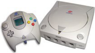
273
based on PowerVR, and the VideoLogic Systems division created branded PC
boards using those chips. PowerVR Series1 products, the PCX1 and PCX2,
introduced in 1996 and 1997 respectively, were available as the OEM
graphics on some Compaq PC models, and as PCI cards from vendors such
as Matrox.
PowerVR Series2, also developed with NEC, was integrated in Sega’s
Dreamcast console, which was released in Japan in November 1998, as well
as in Sega’s Naomi arcade system. Naomi games found in arcades at the
time included House of the Dead 2 from Sega and Power Stone from
Capcom. By 1999, NEC had shipped over one million PowerVR 2DC
chips to Sega for use in the Dreamcast and Naomi systems.
Sega Dreamcast console, circa 1998.
There were also PowerVR Series2 products for the PC (Neon 250
graphics accelerator) and arcade (as well as Sega’s Naomi and Naomi2,
there was the R-Cade Vision 250 for the ArcadePC platform).
A strategic relationship with STMicroelectronics announced in 1999 was
instrumental in bringing PowerVR technology into dozens of new
products. ST’s KYRO, announced a year later, was the first full-featured
PC graphics and video accelerator based on Imagination’s PowerVR
Series3 technology. Using TBDR technology, KYRO and KYRO II chips
provided excellent image quality and a complete modern feature set at a
reasonable cost, enabling developers to create rich environments at high
frame rates.
274
In 1999, the PowerVR 2D/3D graphics processor design was granted
Millennium Products status, announced by Britain’s Prime Minister Tony
Blair as part of the Design Council’s Millennium Products initiative.
A Change in Business Model
By 1999, Imagination was creating a large number of innovative
technologies and decided to make these available to the wider market.
Under the leadership of CEO Hossein Yassaie, the company formally
refocused on intellectual property licensing and changed its name to
Imagination Technologies to better reflect the company’s activities.
Consequently, the company was split into two operating business units.
The PowerVR Technology division developed and marketed PowerVR
graphics/video technology, and the VideoLogic Systems division
produced a range of innovative and award-winning products in the areas
of 2D/3D graphics and sound acceleration, home audio systems, electronic
music, DVD, digital entertainment, video-capture, and video-conferencing.
VideoLogic’s consumer product brand soon became Pure Digital and was
soon simply called Pure. Over time, Pure has become a world-leading
consumer electronics manufacturer, leading the way in mainstream wireless
music and radio systems and entertainment cloud services as well as
innovating in new areas such as TV set-top boxes with advanced graphical
UIs.
Imagination was awarded the title of 1999 Company of the Year in the
prestigious PLC Awards, sponsored by PricewaterhouseCoopers in
association with The London Stock Exchange and the Financial Times.
The award recognized Imagination for its strong management and long-
term strategy. A short time later, in April 2000, Imagination was awarded
two Queen’s Awards for Enterprise. The Awards for Enterprise Innovation
and International Trade were presented to the company’s PowerVR
Technologies division.
275
Enabling the Mobile Graphics Revolution
Around that time, the company announced another long-ranging
strategic decision: it would take its PowerVR architecture into mobile
devices.
While even the best mobile computing devices of the late 1990s had little
graphical capability, the company was convinced that its technology, which
had been designed for low power, could enable a revolution in mobile
visual applications.
With innovative differentiators such as TBDR, as well as a low memory
bandwidth and low-power advantages, Imagination’s PowerVR GPUs were
well positioned to lead the mobile graphics revolution. A number of
strategic partnerships beginning in early 2001, as well as a new product
family, PowerVR MBX, which also launched that year, set the stage.
PowerVR MBX was a complete 2D/3D graphics solution for wireless
multimedia devices, with two variants—MBX, which was optimized for
speed, and MBX Lite, which was optimized for low power consumption.
PowerVR MBX was Imagination’s first PowerVR core for mobile devices
that included support for the company’s proprietary PVRTC texture
compression technology. PVRTC significantly decreased the memory
footprint associated with texture mapping in GPUs.
Initial MBX mobile licensees included Hitachi, Renesas, and TI. MBX
was a vital component of the STMicroelectronics Pocket Multimedia (PMM)
platform. Numerous other leading semiconductor companies soon
followed, with the platform being licensed by seven of the top ten
semiconductor manufacturers at the time.
In 2002, Imagination created Imagination Technologies KK in Tokyo to
enable it to exploit further opportunities with Japan’s consumer electronics
and semiconductor companies. Other major licensees joined with
Imagination around this time to proliferate Imagination’s technologies into
new areas. New broad-ranging license agreements were announced in 2002
with companies including Intel and Frontier Silicon.
276
Key strategic partners supporting the proliferation of PowerVR included HI
Corp., Connect Technologies, and ARM. Imagination also joined the
Khronos Group as a promoter member in 2002 to drive the development
of open standard APIs which allow manufacturers to leverage new graphics
capabilities, such as those found in the PowerVR MBX core.
A Broader IP Portfolio
While PowerVR was driving the creation of entirely new categories of
mobile products, Imagination’s CEO Yassaie was already thinking beyond
graphics to providing larger system solutions. In 2000, Imagination
acquired Ensigma, a fourteen-year-old private company specializing in
Digital Signal Processing (DSP). With Ensigma, Imagination gained
expertise and state-of-the-art algorithms in the key areas of audio and
speech processing for wireless and Internet communication.
In 2001, Imagination further extended DSP technologies with the launch
of Metagence Technologies (‘Metagence’ was later shortened to ‘Meta’) and
also purchased Cross Products Limited, a company that designed and
produced CodeScape development tools for processors.
The Metagence processor architecture leveraged multi-threading to run
several real-time tasks on a single processor, rather than using inefficient
multi-DSP solutions. The first processor based on the Metagence
architecture was the META-1 core. It was integrated into Frontier Silicon’s
Chorus FS1010, a single-chip Digital Audio Broadcasting (DAB)/audio
processor that also incorporated receiver technologies developed by the
Ensigma team. The first product to use the Chorus FS1010 chip was Pure’s
highly popular sub-£99 EVOKE-1 radio in 2002.

277
Pure’s highly popular sub-£99 EVOKE-1 radio, circa 2002.
The same chip was used in Pure’s products up until about 2005 and was
also used in hundreds of other digital radio products from other
manufacturers. Later Pure products used follow-on versions of the Chorus
SoCs, with newer versions of Meta and Ensigma technologies.
Over time, Meta continued to evolve, getting a floating-point unit, higher
clock speeds, Linux and Android support and more. As of 2013, Meta had
evolved into a leading audio platform that is embedded in numerous
generations of products. Meta is also used in many of Imagination’s IP
platforms for video and communications. The Ensigma technologies have
also continued to evolve, and have gone on to ship in tens of millions of
devices. CodeScape continues as Imagination’s comprehensive suite of
development tools, which supports the advanced and unique features of
Imagination’s programmable IP cores.
2005: A Banner Year for PowerVR Graphics and Video
The year 2005 marked a major milestone with the introduction of the
PowerVR SGX GPU architecture. The first implementation of PowerVR
SGX was Imagination’s PowerVR Series5 scalable and fully programmable
multi-threaded universal shader graphics core family. The first SGX cores

278
targeted mainstream and high-performance mobile graphics with state-of-
the-art support for 2D and 3D and a feature set that exceeded OpenGL ES
2.0 shader and Microsoft Vertex and Pixel Shader Model 3 requirements.
Shaders are advanced effects applied to the graphics image that enable more
realistic images to be created. Unlike traditional 3D rendering, shaders are
programmable, enabling the content developers’ creativity to become the
defining factor on how a game, UI or application looks.
2005 also marked the introduction of PowerVR video encoder and
decoder IP cores. Since then, the company has introduced five generations of
PowerVR VPUs (video processing units), comprised of a balance of hard-
coded and programmable elements that combine to deliver efficient multi-
standard and multi-stream video decoders and encoders. As of 2013,
Imagination’s PowerVR video IP had shipped over 600 million units.
PowerVR Graphics Leadership
PowerVR graphics continued to proliferate, and the industry took notice.
In 2006, both Intel and Apple invested in Imagination, and the companies
have continued to be significant stakeholders in the company. By the end
of 2006, there were more than thirty handsets in production from a range
of vendors using PowerVR GPUs, including handsets from NEC, Nokia,
NTT Docomo, Panasonic, Samsung, Sharp, and Sony Ericsson.
PowerVR’s progress and innovation continued unabated. In 2007,
Imagination demonstrated the first OpenGL ES 2.0 silicon. By 2008,
PowerVR graphics were the de facto standard in mobile graphics, reaching a
279
milestone of having been shipped in over 100 million consumer products.
The 200 million unit milestone was reached in 2009. A quarter of a billion
PowerVR-enabled devices shipped as of 2010. As of 2013, PowerVR
graphics had shipped in over 1 billion devices, making it the most
successful graphics technology for mobile and embedded applications.
In 2012 Imagination introduced its latest generation of PowerVR
graphics processors. The PowerVR Series6 ‘Rogue’ GPU architecture was
built on the maturity and success of the previous five generations of
PowerVR graphics IP cores. The PowerVR Series6 GPUs are based on a
scalable number of compute clusters, arrays of programmable computing
elements designed to offer high performance and efficiency while
minimizing power and bandwidth requirements, with an architecture
approximately 5x more efficient than previous generations.
PowerVR GPUs are also capable of doing more than just graphics. By
supporting compute-based APIs such as OpenCL, Renderscript and
Filterscript, the PowerVR architecture delivers vast parallel processing
power, increasingly referred to as ‘GPU compute.’ Using this technology,
GPUs will increasingly come to dominate ‘heavy lifting’ processor-
intensive computing as part of heterogeneous SoCs.
With this in mind, in 2012, Imagination joined the Heterogeneous System
Architecture (HSA) Foundation as a founder member, together with AMD,
ARM, MediaTek, Qualcomm, Texas Instruments, and Samsung. The HSA
Foundation is a non-profit consortium focused on defining and providing
an open, standards-based approach to heterogeneous computing.
PowerVR Developers
Imagination’s public Graphics SDK (Software Development Kit), first
introduced in 2001, played a key role in PowerVR adoption. Designed to
enable all software developers to produce games, applications and utilities
optimized for PowerVR, the SDK enabled developers to learn by example
how to get the best from PowerVR. The SDK has been updated and
280
innovated over time to enable developers to take full advantage of the
growing capabilities of PowerVR.
With the launch of the PowerVR Insider program in 2005 and the
addition of a comprehensive PowerVR Insider online resource for
developers in 2006, the Imagination developer program continued to
grow. Today the PowerVR Insider SDK is a cross-platform toolkit designed
to support all aspects of 3D graphics application development, specializing
in support for devices that contain PowerVR GPUs and enabling users to
get the most out of the graphics acceleration hardware available to them.
In 2013, the PowerVR Insider community had more than 40,000 members.
A Growing Portfolio of SoC IP
Over time, Imagination has continued to set the pace in a range of technologies,
bringing to market new microprocessor, DSP, communications, and video
technologies, with a focus on high performance, power efficiency and
multi-standard capability across its range of IP offerings.
In 2010, Imagination announced that it was bringing to market its Flow
portfolio of enabling technologies for cloud connectivity. The Flow
technology had already experienced success in powering the Pure division’s
market-leading Flow range of connected audio products.
Today, Imagination’s FlowCloud technology includes highly-integrated
licensable hardware based on Imagination’s market-leading silicon IP and
supporting software solutions, complemented by a range of internet-based
technologies and a portfolio of cloud-based resources and services together
with access to an extensive and growing ecosystem of partners’ services and
content.
In addition to adding capabilities to its existing IP portfolio, the company
also looked for continued areas of expansion. In 2010, Imagination
acquired two new companies. First was HelloSoft, one of the world’s
leading providers of Video and Voice over Internet Protocol (V.VoIP) and
wireless LAN technologies. This acquisition addressed the key requirement
281
for network operators in the 4G age to ensure devices can access all
different networks, with varied connecting technologies.
Imagination’s second 2010 acquisition was Caustic Graphics, a developer of
hardware/software real-time ray-tracing graphics technology. Ray tracing is
a technique for rendering cinema-quality 3D at a level of near-photographic
realism that is impractical with traditional 3D graphics techniques. As of
2013, Imagination offers this technology in Caustic Professional ray tracing
PC boards for content creation professionals, with plans to provide the
technology in IP form in the future.
The company’s technology portfolio continued to expand with the 2012
acquisition of Nethra Imaging, a semiconductor and systems company
focused on delivering video and imaging solutions. With the addition of
these technologies, Imagination continued its focus on building a total
solutions portfolio for future SoC designs.
Popular MIPS Architecture Comes to Imagination
In 2013, Imagination completed its acquisition of MIPS Technologies.
With MIPS, Imagination added to its IP portfolio one of the most prolific,
longest-living processor architectures, greatly enhancing the company’s
CPU offerings and roadmap.
Over more than three decades, MIPS has powered
products including game systems from Nintendo
and Sony; DVRs from Dish Network, EchoStar, and
TiVo; set-top boxes from Cisco and Motorola;
DTVs from Samsung and LG; routers from Cisco,
NetGear, and Linksys; automobiles from Toyota,
Volvo, Lexus, and Cadillac; printers from HP,
Brother, and Ricoh; digital cameras from Canon, Samsung, FujiFilm, Sony,
Kodak, Nikon, Pentax, and Olympus; and countless others. MIPS licensees
have shipped more than 3.5 billion units since 2000.
At the heart of MIPS is a pure RISC (reduced instruction set computing)
instruction set, a clean and elegant solution that leads to lower power
282
consumption and smaller silicon area than other CPUs. MIPS processors
feature advanced technologies such as hardware multi-threading,
compatible 32-bit and 64-bit instruction set architectures (ISAs), and ISA
consistency from entry-level to high-end.
Continuing Innovation
CEO Hossein Yassaie was awarded a knighthood in the 2013 New Year
Honors. The award was given in recognition of his services to technology
and innovation.
In 2013, the company began preparing for the next stage of its growth,
focused on total SoC solutions. With PowerVR graphics and video, this
includes support for 4K ultra-HD video technologies, driving GPU
compute applications, and enabling the next generation of 3D graphics
technology with ray tracing. It also includes enabling low-power, multi-
standard connectivity with Ensigma radio processors (RPUs), providing
the industry’s highest quality of service for V.VoIP and VoLTE through its
HelloSoft IP and leveraging the company’s FlowCloud technology to
enable seamless delivery of services and content between service providers
and users through the cloud. Another key strategic initiative is in driving
MIPS CPUs to become a leading force in the market.
Innovation also continues in the Pure consumer electronics (CE)
division. Building on the strong foundation of its success in radio, Pure has
been driving product and platform developments that significantly broaden
its market reach to include wireless streaming and internet-connected
audio, broadcast radio, in-car radio and audio, cloud-based services and
connected set-top boxes. Pure is also key to Imagination’s partnerships in
entertainment and content. In 2012, Pure engaged with Onkyo, VW group,
Universal Music Group, Alpine and Pioneer, helping to consolidate
Imagination as a significant voice in entertainment technologies.
283
Imagination leveraged its audio expertise in the development and 2013
launch of Caskeid, a technology that delivers exceptionally accurate
synchronized wireless multiroom connected audio streaming. Pure’s Jongo
system is the first Caskeid-enabled multiroom system to deliver the sync
performance and quality of a wired system in a wireless setting. Caskeid
works seamlessly with Imagination’s FlowAudio cloud-based music and
radio service which delivers access to over 22 million music tracks as well
as hundreds of thousands of radio stations, on-demand programs and
podcasts.
Imagination House at the company’s headquarters in King’s Langley, Hertfordshire,
UK.
The “Market Share Analysis: Semiconductor Design Intellectual
Property, Worldwide, 2012” report from market research firm Gartner
showed that the third-party semiconductor design IP market grew by
11.2% in 2012, and in that same period, Imagination grew by 36.4%. MIPS
Technologies, recently acquired by Imagination, also outpaced industry
growth in 2012, growing by more than 17%. For the sixth year in a row,
Imagination maintained its position in the survey as the third-largest design
IP provider, with its overall share growing each year. With MIPS in the
fourth position, the companies together comprised 11.3% of the design IP
market share. As of June 2013, Imagination IP has cumulatively shipped in
284
over 5 billion devices, with many of those devices containing more than
one of Imagination’s technologies.
285
2019 Update: Wave Computing
and MIPS Technologies
Wave Computing, a Silicon Valley-based artificial intelligence company
specializing in dataflow-based processing, acquired MIPS Technologies for
an undisclosed amount in July 2018. Not only was this union projected to
make Wave Computing immediately cash-flow positive, but it opened new
markets such as edge AI computing, while giving the company in-house
RISC cores it could use for its next-generation DataFlow Processing Unit
(DPU) chips, known as WaveFlow technology. The MIPS acquisition also
became a critical factor contributing to Wave Computing’s vision for
delivering artificial intelligence acceleration from the data center to the
edge.
MIPS has been a key player in multithreaded, power efficient processors,
driving smart edge and autonomous devices for more than 25 years. MIPS
processors power 80 percent of today’s Advanced Driver Assistance
Systems (ADAS)-enabled vehicles from leading auto manufacturers such
as Toyota, Volvo, Lexus and AUDI. They can also be found in Cisco,
Netgear and Linksys routers; Nintendo and Sony gaming systems; Canon,
Nikon, Fujifilm, Pentax and Olympus cameras; Cisco and Motorola set-top
boxes; and Samsung and LG DTV’s.
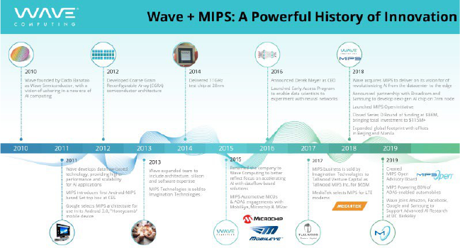
286
From Here to Eternity and Back Again
MIPS Technologies, formerly MIPS Computing, has one of the longest,
most iconic and prolific histories in semiconductor IP. It extends over three
decades—an eternity in the PC/Internet age. MIPS has been major player,
driving some of the most powerful servers and workstations on the market,
including those from Silicon Graphics Inc. (SGI) that generated Hollywood
special effects for such breakthrough ‘90s blockbuster movies like Jurassic
Park.
Pioneered by Stanford University professor, John Hennessy, in the early
1980s, MIPS’s Reduced Instruction Set Computing Design (RISC) was a
radical idea in its time, replacing the increasingly complex instructions
common at the time with much simpler instructions that would enable
easier pipelining, larger caches, lower power requirements and fast
performance. MIPS was also the first company on the market with a 64-bit
processor.
SGI acquired MIPS Computing in 1992 and ran it as a wholly-owned
subsidiary, which it retitled as MIPS Technologies, Inc. SGI spun out MIPS
as a stand-alone IP company, which Derek Meyer—who later became
287
CEO of Wave Computing—took public in 1998 with a focus on catering
to the embedded market for 3D-graphics that arose from the increasing use
of Apple Macintoshes and Intel-based PCs.
The Move to the Edge
Several MIPS innovations came to market between 1998 and 2013, which
is when MIPS was acquired by UK-based Imagination Technologies, a
company known for its PowerVR graphics and video processors. Apple
was a customer for Imagination’s GPU, which was the rumored to be the
most power-efficient GPU available in-market at the time. By acquiring
MIPS Technologies, Imagination hoped to provide both a CPU and GPU
to the mobile computing market; however, it was a little late in the game to
get adequate traction.
Then, in 2014, Imagination formed a partnership with leading ADAS
provider MobilEye, to provide reliable, efficient vision processing for
MobilEye’s ADAS technology for automobiles. MobilEye leveraged
MIPS’s multithreaded microAptiv cores and Series 5 Warrior cores to
provide the real-time response capabilities, Quality of Service and reliability
necessary to perform multiple operations simultaneously across several
embedded Vision Processors. With this technology, MobilEye became a
critical part of in-vehicle, ADAS systems for more than 27 car
manufacturers around the world.
In 2015, MIPS formed the MIPS Academy, a program through which
the company made its instruction set architecture (ISA) and other tools
available for free to a global ecosystem of 670 students and faculty at 44
different universities around the world. Later that same year, Imagination
entered into a strategic partnership with PEZY, a Japan-based processor
company, to integrate Imagination’s highly efficient 64-bit MIPS Warrior
CPUs in its next-generation PEZY-SC2 many-core processors for
supercomputers and other high-performance applications.
288
The next big customer win for MIPS came in the fall of 2017 when
MediaTek, a leading fabless semiconductor company for wireless
communications and digital multimedia solutions, adopted multi-threaded
MIPS I-class CPUs for smartphone LTE modems. The first device from
MediaTek featuring MIPS technology was the flagship MT6799 Helio™
X30 processor, which uses MIPS in its Cat-10 LTE modem. The
relationship with MediaTek catapulted MIPS into the high-volume
smartphone and modem market, a testament to the performance and
efficiency advantages MIPS’ multi-threading technology delivered for real-
time, power sensitive applications such as mobile, artificial intelligence and
Internet of Things applications.
Safety Advances Launch MIPS Into Automotive
In 2016 Imagination released the MIPS i6500 line of cores, a family of
64-bit multithreaded, multi-core, multi-cluster processors that were later
validated to meet automotive functional safety (FuSA) compliance
standards. Multi-threading technology allowed different analyses and
decision-making on each thread for real-time safety-critical situations, such
as analyzing a pedestrian’s height, motion, and shadow to anticipate
whether he or she was about to cross the street. FuSa was critical to all parts
of an auto’s safety-critical system, including any CPUs being used in the
vehicle’s AI System on a Chip (SoC) sockets.
Then, in 2017, Imagination collaborated with Barco Silex, a global leader
in security IP cores and platforms, to develop IP for secure SoC platforms
based on MIPS processor families. Barco utilized the MIPS microAptiv
CPU, an ultra-low power controller, for its embedded eSecure system,
guaranteeing the authenticity and integrity of an embedded application’s
hardware, software, data, and communication. This partnership boosted
MIPS’s portfolio of processors offering safety and intelligence to “smart,
safe and secure cores.”
289
Under the agreement, Imagination integrated Barco Silex’ eSecure
solution for embedded security into a new Trusted Element (TE) IP
product, which it then licensed to help customers enhance the security of
a diverse set of use cases ranging from data center equipment to low-power
IoT wireless sensor nodes.
Delivering AI from the Datacenter to the Edge
All artificial intelligence applications need to conduct both model training
and data inferencing to provide ‘outcomes’ or instructions that guide what
action needs to be taken. There are two major locations where this model
training and data inferencing take place—both in the data center (or ‘the
cloud’) and in ‘edge’ devices such as smart cars, AI-enabled personal
assistants, modems, FitBits, etc. The myriad and multitude of edge devices
at use in society today capture up to petabytes of data every day. It’s due to
the sheer volume of information captured by these edge devices that it
becomes necessary to share it back with data center processing
environments, allowing AI algorithms or models to process and analyze
that data in batch form to make longer-term, consistent recommendations.
The explosion of data capture and the rate at which intelligent decisions
must be made is what’s driving the demand to connect AI processes and
architectures from the data center out to the edge.
Wave Computing, an emerging player in specialized processors for
artificial intelligence and deep learning networks, acquired MIPS in June
2018. With the MIPS acquisition, Wave sought to combine its WaveFlow™
technology with core designs from MIPS to offer a common AI
architecture that could scale from the data center to the edge. The
applications include autonomous vehicles, in-dash, vehicle technology that
alerts the driver to a car in their blind spot to prevent them from changing
lanes; a security sensor or camera that identifies an intruder and sets off an
alarm, dials the local police and automatically locks all doors or windows;
an intelligent system that processes video streams to determine sentiment
290
of thousands of shoppers as they stroll through megamalls or superstores,
enabling retailers to make more intelligent marketing campaigns or
merchandise placement.
Wave Computing’s unique approach to Dataflow applications—known
as WaveFlow™—aims to accelerate training and processing of deep neural
networks for artificial intelligence without any CPU intervention. It’s an
elegant, scalable alternative to more traditional data center AI architectures
that employ GPU’s in combination with CPUs. By combining its power-
efficient, multithreaded, MIPS RISC processors with its WaveFlow-based
systems and software technology, Wave Computing delivers a scalable,
end-to-end AI platform capable of addressing all configuration, power,
intelligence, and safety requirements needed to make the use of AI more
pervasive throughout society.
291
2019 Update: IP Management
As RTL design started to increase in the late 1980s and early 1990s, it
was becoming apparent that some amount of management was needed to
keep track of all the design files and their associated versions. Because of
the parallels to software development, design teams looked to the tools and
methodologies that were in use by software teams at the time.
Software teams had adopted Software Configuration Management
solutions to handle the organization and versioning of their source code.
RCS and CVS were two of the most popular revision control systems in
use at the time, and semiconductor development teams began to adopt
these for their development environment, eventually building
methodologies around the use of these solutions.
It quickly became apparent that the differences between hardware and
software design necessitated the development of more customized
solutions for the semiconductor development teams. Binary databases for
analog design needed to be supported, along with integration into the EDA
environment, and support for scripting and configuration files for the EDA
tool flow.
In 1993, the consulting group at VIEWLogic began work on providing
the first such environment for hardware teams. Building on top of RCS,
they released ViewData, a plugin for the PowerView framework. This
solution began to address the needs of managing configurations of files
where RTL, schematics, and layout all made up the final design
configuration.
292
In 1995, Dennis Harmon, Mitch Mastelone, Norm Sozio, and Eugene
Connolly left VIEWLogic to form Synchronicity with the goal of providing
the first true semiconductor design data management system that would
manage design data across different development platforms and EDA tool
environments. In 1996, they released DesignSync, which was built on top
of a custom data management system that could handle the RTL and other
ASCII data, and connectors into the solution that would interface with the
EDA tools at the time. This solution became popular with analog designers,
as now there was a way to handle the binary data and custom frameworks
associated with Analog design.
Two years later, Srinath Anantharaman founded ClioSoft to continue to
fill in the gaps that were not met by software SCM tools. ClioSoft launched
the SOS design collaboration platform to target the challenges of hardware
design. Like DesignSync, ClioSoft built SOS on top of a customized data
management system and developed technology to augment the traditional
SCM approach to create a hardware configuration management (HCM)
system while partnering with EDA companies to provide specific
connectors into the EDA tools and methodologies.
In the ensuing years, there was a rise in the development of commercially
available data management (DM) platforms. IBM Rational’s ClearCase and
Perforce’s Helix were being adopted by development teams in many
different industries. A new generation of open source solutions was also
being developed, such as Subversion and later, Git. This allowed for a
second generation of solutions to be introduced to the market that allowed
for the adoption of solutions that were built on top of these commercially
available solutions instead of running on proprietary data management
systems.
In 2003, Shiv Shikland and Dean Drako founded IC Manage. Building
on top of Perforce’s Helix data management solution, they released their
Global Design Platform (GDP). By choosing to release their solution on
top of a commercially available DM system, design teams were able to use
293
a common DM system for software and hardware design, with the GDP
client able to be customized for the needs of hardware designers.
Four years later, Simon Butler and Fergus Slorach founded Methodics.
Methodics also chose to run on top of commercially available systems, but
instead of limiting the solution to a single platform, they chose to allow
users to run their choice of platforms, with Perforce and Subversion being
the two most popular at the time. This further allowed customers to mix
and match backend DM systems to fit their needs while having a common
client, VersIC, running on top of the different systems for hardware design.
As design reuse began to gain traction in the early 2000s and the use of
third-party IP began to grow, semiconductor designers were now faced
with the challenge of managing designs for reuse, and managing the
acquisition of third-party IP. Design teams needed to know where to find
internal IP for reuse and be able to track what versions were being used, in
which projects it was being used in, and what products had taped out with
what versions of IP. Third-party IP complicated the problem, as each IP
acquired often had a different contract that stipulated how the IP provider
was to be paid for the IP’s use. Often, users of this IP would have to keep
track of varying business terms that required the users to keep track of who
looked at the IP, was it uses once or many times in a design, how many
different designs was it used in, or how many parts were ultimately shipped
after tapeout.
Semiconductor design teams looked to the design management companies
to provide solutions in this area. Synchronicity was first to market in the IP
management space with IP Gear, Methodics released ProjectIC, IC Manage
developed IP Central, and ClioSoft released DesignHub. Later, in 2004,
Synchronicity would be acquired by MatrixOne, developer of one of the first
PLM systems, to bring semiconductor design management closer to systems
development. MatrixOne would then be acquired by Dassault Systèmes in
2006. While DesignSync lives on as part of the ENOVIA PLM group inside
of Dassault, IP management has been integrated into the ENOVIA PLM
294
platform itself. Methodics has release Percipient as a follow on to ProjectIC,
incorporating an IP LifeCycle Management (IPLM) methodology into the
solution and providing integration to other engineering systems like
requirements management and issue and defect systems.
Today, SoCs continue to take advantage of reuse, with the number of IP
cores in an SoC exceeding 100. The challenges facing the management of
IP are still increasing. Functional safety requirements, such as ISO 26262
for automotive and DO-254 for aerospace, push semiconductor companies
to provide evidence of a traceable path from requirements through design
to verification and to document all work that has been done to meet those
requirements. The need for these traceable flows requires that IP
management systems have links into requirements, verification, and
document management systems. Increasing use of third-party IP is making
designers look for robust IP portals with abundant IP metadata available
so that they can accurately compare IP from different vendors. With the
industries dependence now on IP, IP management systems will remain core
to the effective collaboration of design teams for the years to come.
295
In Their Own Words: Methodics
Methodics has been a key player in IP management for over 10 years. In
this section, Methodics shares its history, technology, and its role in
developing IP Lifecycle Management (IPLM) solutions for the electronics
industry.
Methodics is recognized as a premier provider of IP Lifecycle
Management (IPLM) and traceability solutions for the Enterprise.
Methodics solutions allow semiconductor design teams to benefit from the
solutions ability to enable high-performance analog/mixed-signal, digital,
software, and SOC design collaboration across multi-site and multi-
geographic design teams and to track the usage of their important design
assets.
The journey started in 2006 when Methodics was founded in 2006 by
two ex-Cadence experts in the Custom IC design tools space, Simon Butler
and Fergus Slorach. After leaving Cadence, they started a consulting
company called IC Methods, active in Silicon Valley from 2000-2006. As
their consulting business grew, they needed to create a new company to
service an engagement that had turned into a product for analog data
management. With IP management in their DNA, They reused the IP in
their consulting company name and Methodics was born! Methodics first
customer was Netlogic Microsystems, which was later acquired by
Broadcom. Netlogic used the first commercial product developed by
Methodics, VersIC, which provides analog design data management for
Cadence Virtuoso. The development of Virtuoso was unique in that
296
Methodics did not have to also develop an underlying data management
layer as the first-generation design data management companies in the
semiconductor industry had to. During the late 1990s and early 2000s, a
number of data management solutions had entered the market. Some of
these solutions were open-source, such as Subversion, and others were
commercially available, like Perforce. These solutions had developed very
robust data management offerings and were in use by 100,000s of users in
multiple industries.
To leverage these successful data management solutions, Methodics
made the architectural decision to build a client layer on top of these
products, allowing the team to focus its engineering efforts on developing
a unique and full-featured client, and not having to develop and maintain a
layer for the design data management. Customers would benefit from this
arrangement by having a full-featured client integrated directly into the
Virtuoso environment, and also have a robust data management layer that
was widely in use, without necessarily having to concern themselves with
the ongoings of the data management system.
It wasn’t too long before Methodics' customers started asking for a
solution that could be used in the digital domain as well. With the increase
of companies adopting design reuse methodologies and using third-party
IP, Methodics decided to not only deliver a solution for digital design, but
also one that could be used to manage and track IP reuse throughout their
companies. This led to the development of ProjectIC, which could be used
not only for digital design, but analog design as well.
ProjectIC was an enterprise solution for releasing IP’s and cataloging them
for reuse, SoC integration, tracking bugs across IP’s and managing
permissions. ProjectIC also allowed for the comprehensive auditing of IP
usage and user workspaces. With ProjectIC managers could assemble
configurations of qualified releases as part of the larger SoC and make this
available for designers to build their workspaces. Workspace management
was a key technology within ProjectIC as well, and Methodics created a
297
caching function to allow data to be populated in minimal time. Like VersIC
before it, ProjectIC was built on top of the growing number of solutions
available for data management, which allowed customers to quickly integrate
to their development methodologies, especially if design teams had already
adopted a commercially available system for data management.
In 2012, Methodics acquired Missing Link Software, which had
developed Evolve, a test, regressions and release management tool focused
on the digital space. Evolve tracked the entire design test history and
provided audit capabilities on what tests were run, when and by whom.
These were associated with DM releases and provided a way to gate releases
based on the required quality for that point in the designs’ schedule.
With the acquisition of Missing Link, Methodics began to focus on the
traceability of design information throughout the entire development
process. While the core solutions of Methodics could keep track of who
was developing IP, who was using which releases in which designs, and
what designs were taped out using specific releases, the customer wanted
even more visibility into the life cycle of the IP. They wanted to know what
requirements were used in developing IP, whether it was internally
developed or acquired, what versions of the IP incorporated which features
based on requirements, and how that IP was tested, verified, and integrated
into the design. What was needed by customers was not only an IP
management solution, but a methodology that could be adopted to track
the lifecycle of an IP.
In 2017, Methodics released the Percipient platform, the second
generation IP Lifecycle Management solution. Percipient built on the
success of ProjectIC, but also began to allow for integrations into other
engineering systems. In order to fully track an IP’s lifecycle, Percipient
created integrations into requirements management systems, issue and
defect systems, program and project management systems, and test
management systems. These integrations allow for a fully traceable
environment, from requirements, through design, to verification, of the
298
lifecycle of an IP. Users of the Percipient platform can now not only track
where an IP is used and which version is being used, but can now see what
requirements were used in the development of an IP, any outstanding
issues that IP might have and what other projects are affected, and whether
the IP is meeting requirements based on current verification information.
Today, Methodics continues to develop solutions for fully traceable IP
lifecycle management as well as solutions for mission-critical industries that
require strict adherence to functional safety requirements like automotive
and ISO 26262 and Aerospace DO-254. Methodics is also working on
solutions to increase engineering productivity. With workspaces growing
exponentially, Methodics is developing solutions like WarpStor, which
virtualizes engineering workspaces and drastically reduces data storage
requirements while increasing network bandwidth. With the adoption of
cloud computing by semiconductor companies, Methodics is also working
on solutions to help customers work with hybrid compute environments
of on-premise and cloud-based. Just as it was in 2006, Methodics goal is to
bring value engineering teams by making the development environment
more efficient by enabling close collaboration and the optimization of
resources.
299
Chapter 8: What’s Next for the
Semiconductor Industry?
In 2019, we are in the midst of another transition in the semiconductor
industry. Several factors are causing the change: 1) Competitive
consolidation at 7 nm for IDMs and foundry suppliers, 2) Entry of systems
companies, especially automotive and information technology, into the
world of integrated circuit design and 3) Massive investment by China to
become self-sufficient in semiconductors.
Silicon Foundries – Phase 3
The silicon foundry supply system has evolved substantially since the
early 1980s when Seiko Epson was a leading supplier, and customers like
Chips & Technologies took advantage of spare capacity at major
semiconductor companies like NEC. Even Intel announced that it would
enter the foundry business in 1981 but quickly changed direction when the
PC-driven boom of 1983 through 1984 took off, straining existing capacity.
In the next phase, companies like TSMC, UMC, and others made
substantial investments in capacity and communicated their willingness to
support fabless semiconductor companies with standard processes. TSMC
was uniquely visible as a pure foundry, offering no products of its own, and
emphasizing its dedication to avoid competing with its customers. UMC
continued to build ROMs and static RAMs to keep the fab full, and Morris
Chang was Chairman of both companies. Perhaps most innovative was the
decision by TSMC to make its design rules generally available rather than
300
hiding them under a veil of secrecy with strict non-disclosure agreements.
This provided a process standardization for customers and was helped
along by the VLSI Technology Passport Library that facilitated some
degree of design portability. The success of the TSMC approach is well
documented in this book. Total foundry output now approaches 20% of
all IC production and is nearly 30% of the non-memory wafers produced.
In 2018, we began the Phase 3 transition that sets the basis for the
coming years. By this time, it became clear that leading foundries, especially
TSMC and Samsung, could not only match the process capability of
integrated device manufacturers but could actually exceed it. This was
helped by delays of the Intel “10 nm” process (which was roughly
equivalent to the TSMC and Samsung “7 nm” processes). At this point,
companies like AMD could develop processors with competitive design
rules and manufacture them in foundries, avoiding the growing cost of
semiconductor capital equipment and investment in semiconductor
process technology.
This Phase 3 saw the shake-out of foundry suppliers. In late 2018,
GLOBALFOUNDRIES announced that it was terminating its
development of 7 nm technology and would focus on differentiated
processes including FDSOI. SMIC was not intimidated by the cost and
competition of future technology nodes, announcing that its 14 nm process
would be in volume production in the first half of 2019 and that it would
continue to the future nodes.
What’s likely to happen? In the coming years, it’s reasonable to expect
that very few foundries will be able to afford the cost of process
development beyond 7 nm. Certainly, TSMC and probably Samsung will
continue. SMIC has the financial capacity to catch this wave as well. For
the time being, it’s doubtful that more foundries will appear at the leading
edge. Political pressures that are driving China may drive the U.S. as well
because of concern about the dependence of the U.S. electronics industry
on the supply of wafers from Asia. Most likely, future concerns about the
301
geographic concentration of advanced semiconductor foundry technology
in Asia will lead to more aggressive installation of advanced capacity in the
U.S., and maybe Europe, by either TSMC or Samsung or both.
For the IDMs, Intel and Samsung are clearly committed to continuing to
develop processes with smaller feature sizes and advanced capabilities.
Memory companies like SK Hynix, Micron, Samsung and new Chinese
entrants will probably do the same for DRAM, but NAND FLASH can be
produced at lagging design rules because of die stacking which may very
well go as far as 512 layers.
Increasingly, the silicon foundries are in a race with Outsourced
Semiconductor Assembly and Test providers (OSATs) for the assembly of
components. For many customers, the convenience of a single turnkey
supplier will encourage the move toward wafer level fan-out which the
foundries can dominate. OSATs, however, continue to service the need for
heterogeneous die assembly and test. In the future, the difficulty of
translating data and doing verification in the PCB/module world will
converge via design automation with the wafer level fan-out technologies
so that OSATs can provide competitive alternatives to the silicon
foundries. The packaging world has previously been void of the equivalent
of SDKs and standardized verification flows that characterize the wafer
processing world of foundries. This need is being quickly overcome and
will drive increasing manufacturing process standardization by companies
offering assembly and test services. EDA companies will bridge the
differences in packaging and IC layout standards to make the transfer of
data between the packaging and GDS II environments seamless.
Twenty years down the road, I still expect the specialty foundries to have
a place in the ecosystem. Growth of highly differentiated processes,
adoption of wide bandgap semiconductors like gallium arsenide, gallium
nitride and silicon carbide in applications that involve higher power,
microwave frequencies or other characteristics will enable non-silicon
suppliers to grow their capacity and provide a foundry ecosystem that will
302
stimulate creative design activity by fabless companies. Major foundries are
clearly extending their capabilities into many of these technologies as well,
but there will always be room for specialization.
Systems Companies Join the World of IC Design
The EDA industry has experienced accelerated growth since about 2016
as a whole new set of customers began purchasing advanced EDA
software. Even before this, automotive Tier 1 suppliers, like Bosch and
Denso, began expanding their semiconductor capabilities as their
customers, the automotive OEMs, began to move into areas of traditional
Tier 1 strengths like ECU design and embedded software integration.
Bosch even announced a new wafer fab in 2017.
As enthusiasm for design of electric cars and autonomous driving
capabilities grew, the number of companies designing chips, modules and
software increased. In early 2019 there were nearly 400 companies that have
announced the intention to produce electric cars and light trucks. More
than half of those companies intend to introduce Level 4 or Level 5
autonomous drive capabilities. The traditional automotive industry is
struggling with an identity crisis as cars begin to look more like nodes in a
computer network and the electronic content of vehicles approaches 35%
of the bill of materials cost. Differentiating expertise for the automotive
industry shows some signs of moving from Detroit to Silicon Valley in the
U.S.
Beyond automotive applications, the quest for differentiation in cloud
computing has caused the largest owners of server centers to develop their
own chips, software and PCBs. These include Google, Amazon, Facebook,
Alibaba and many more. Rather than purchase standard servers, these
companies purchase chips and build their own PCBs for their servers.
Moving the differentiation further, they began developing their own chips,
or programming FPGAs, to optimize server performance. They have
become the fastest growing major category of EDA customers and they
use the most advanced design technologies. They were early adopters of
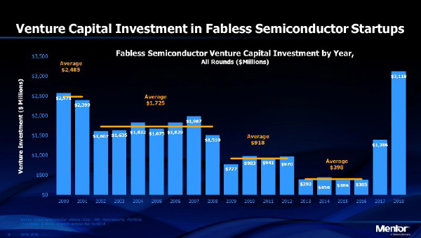
303
the new wave of abstraction in IC design, referred to as “high-level
synthesis.” They now differentiate the data paths of their processors by
developing algorithms in C++ that they automatically synthesize into RTL
(i.e. Verilog, System Verilog or VHDL languages) for the chips. The ability
to formally verify the equivalence of the C++ with the RTL has accelerated
adoption of high-level synthesis.
You might think that we are moving toward a world of big company
design where the cost of designing large, complex chips becomes so great
that only the big companies can afford to compete. Venture capital
investments in fabless semiconductor companies since the “dot com”
boom of the year 2000 have steadily declined from the record level of
$2.5 billion per year to less than $400 million per year in 2016 (Figure 1).
In the second half of 2017, this trend reversed. The year 2018 saw a new
record for venture capital investment in fabless startups at $3.1 billion
dollars, particularly early round startups and those based in China.
Investment in 2019 is on track to set a new record as well. Artificial
intelligence and machine learning drove the majority of these startups but
5G enabling chips also constituted a significant investment.
Figure 1. Venture capital investment in fabless semiconductor companies.
304
How is this evolution going to unfold? There are positives and negatives
for the semiconductor industry.
First, the world does not need 400 companies producing electric cars and
light trucks. There will be a shakeout and, with it, a decrease in the amount
of chip designs and prototypes needed to support the automotive industry.
The same will happen with autonomous driving. 200 companies are far too
many. A handful of companies will provide the central processing and AI
functions that car manufacturers will incorporate in their vehicles through
OEM arrangements. Car companies are already struggling with how to
differentiate their designs as the driving experience becomes less of a
compelling reason for customer choice of a vehicle.
Now the good news for those of us in the semiconductor ecosystem.
Some of the stimulus for accelerated design activity will continue. Demand
for “cloud”, “fog” (gateways) and “mist” (edge node chips and modules)
computing power is likely to grow unabated for the next ten to twenty years
at least. Performance, power and cost challenges will continue, driving high
performance and differentiated technologies.
To a great extent, 5G offers similar growth in semiconductor demand
and new capabilities over the next decade or more. New applications for
artificial intelligence and machine learning should stimulate further
innovation in computer architectures as we develop processors that deviate
from the historical von Neumann approach to one that is more like the
human brain. New domain specific architectures are increasingly
embedding neural network subsystems that facilitate learning of the chips
over time. This experimental period will also lead to a shakeout in the
future. There will likely be a few really big winners in the area of facial
recognition, probably from China where supervised learning can be most
effectively used because of their large database and lack of privacy
restrictions. One would also expect winners in other areas of specialization
as we move to new standard architectures for various applications, different
from the traditional general-purpose computing architectures of today.
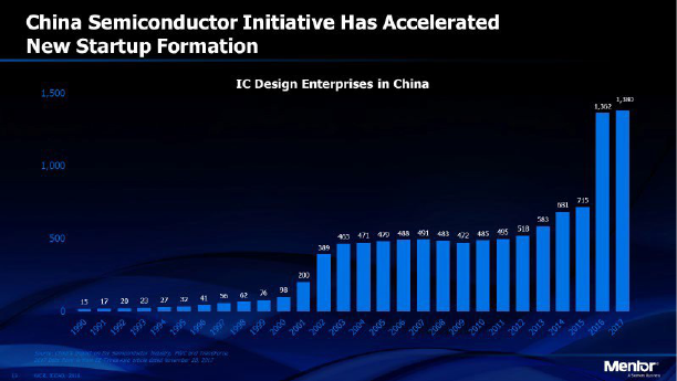
305
China Takes a New Place in the Semiconductor Ecosystem
One of the biggest potential changes in the years ahead is the changing
role of China in the worldwide ecosystem for semiconductors. Chinese
companies have been the largest consumers of integrated circuits in the
world since 2005 but the percentage of those purchases designed or
produced in China has been only 15%. While the Chinese government
has worked to change that situation, a stimulating event that appears to
have accelerated popular resolve in China was the potential destruction of
ZTE when the U.S. placed an embargo on shipments to the company after
there was strong evidence of violation of trade restrictions with Iran. It
then became apparent that the U.S. government had the power to shut
down any, or all, of the Chinese electronics companies. These companies
had become a core part of the Chinese economy as well as a contributor to
military defense, so the threat from the U.S. was not ignored.
The first round of Chinese government stimulus already began before
the ZTE crisis. A government fund of $20 billion was set up. Instead of
directing the investments from a government agency, China injected the
money into semiconductor development via private equity companies, like
Tsinghua Unigroup, who were investing for themselves as well. As it turned
out, this led to a five to one match of the government funds as well as a
disciplined focus on the companies that could be economically successful.
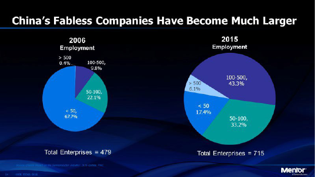
306
Early focus was on manufacturing. More recently, however, the fabless
startups have become a larger share of the investments and that has
stimulated rapid growth in the number of fabless companies in China. The
reported number has increased from about 500 in most of the last fifteen
years to more than 1000 since 2017 (Figure 2)
Figure 2. Reported number of fabless semiconductor companies in China.
The size of these companies has also increased. Figure 3 shows that the
percentage of the fabless semiconductor companies with 100 to 500
employees in 2006 increased from less than 10% to almost 50% in 2015.
Similarly, the number of companies with more than 500 employees
increased from less than 0.5% in 2006 to over 6% in 2015.
Figure 3. Growth in number of employees at Chinese fabless semiconductor
companies.
In 2018, the Chinese government disclosed a new fund with $47 billion
from the government and presumably a significant match from private
equity. Total annual revenue of the worldwide semiconductor industry is
less than $500 billion so this investment is extraordinarily large compared
307
to the revenue opportunity. It represents a strategic objective rather than
just an investment in the future revenue and profitability of the industry.
Will the Chinese government succeed in its objective for self-sufficiency
in semiconductors? It’s doubtful. No country can be totally self-sufficient,
not even the U.S. There will always be some parts of a system that require
innovative solutions from another geography. However, China can become
increasingly self-sufficient in a large share of the total dollars spent on
semiconductors. Willingness to invest a lot of money can lead to
competence, although probably not leadership, in semiconductor memory.
Memory constitutes 30 to 40% of the total semiconductor cost of the
systems.
How else might the Chinese investment affect the future of the
semiconductor ecosystem? Two areas that stand out are artificial
intelligence and 5G wireless communications. Both are heavily influenced
by economies of scale. With 1.4 billion people in China and six cities with
greater than ten million people, the economic advantage for 5G
communications becomes clear. The U.S. doesn’t have enough potential
customers for 5G to make an accelerated investment cost-effective. China
does. And the Chinese government is further stimulating that investment.
A similar but different dynamic exists for Chinese investment in artificial
intelligence. For supervised learning, a large database is a significant
advantage. If you are trying to intelligently diagnose diseases based upon
symptoms and other data from medical tests, then correlation with second-
order effects is more likely to be found with a sample size of one billion
“willing” participants who provide their medical data and histories. The
U.S. and Europe don’t have this opportunity.
I would expect that, in many of these areas, we will see advances in China
that provide government-supported companies with unique capabilities
and semiconductor products. The counter to this is the suppression of
innovation that exists when people are not free to openly communicate
their ideas. Ultimately, the free societies usually win. In the near term,
308
however, we should expect lots of technical advances in semiconductor
capabilities in China that will hopefully stimulate sharing with others
around the world.
Other Factors
Beyond these three trends, there are lots of things happening in the world
of semiconductors that will influence our future. One of the most
interesting changes is the methodology associated with design of chips. We
have used basically the same design methodology since the introduction of
logic synthesis in the late 1980s. It’s only very recently that leaders in the
industry started the move to high-level synthesis, a technology that has
been available for almost twenty years. This change required a new set of
designers and a different type of design problems. Google, nVidia, and a
host of others found that their differentiation was in the data path and they
could improve design time, power and performance by at least 30 to 50%.
A host of other methodologies have been proposed to further reduce
design time, cost and thoroughness of verification. I would expect some
aspects of these approaches to be implemented in the next five years,
ushering in additional innovative designers who can now afford the
entrance fee for developing chips.
Disruption of de facto standard computer architectures is rare and
usually happens only when there is a discontinuity in technology or in the
market. Intel X86 architectures are likely to continue as the leading standard
for servers for a long time but ARM was able to capture the lead in
embedded computing when wireless communications became a
semiconductor growth engine. RISC-V has the potential of capturing the
hearts and minds of a broad range of designers, especially in China, if the
increasing adoption of open source technology creates the opportunity.
One of the most frustrating areas of potential growth is what’s referred
to as the “Internet of Things”. Billions of low power, low-cost chips are
required and yet IoT thus far offers only limited benefit for semiconductor
companies because of just that—ultra-low cost, even at large volumes,
309
leads to limited economic opportunity. Systems companies who can
capture the intellectual property value of an information collection system,
when coupled with the information processing and the sale of the results
of the analysis, have emerged as an increasingly viable path to IoT chip
design and commercialization. With time however, the nodes of the IoT
will acquire additional intelligence as the sophistication of “edge nodes”
increases. That means IoT chips or modules will incorporate analog, digital,
RF, MEMs and other capabilities. Simulating these multi-technology chips
creates challenging opportunities for the most capable designers and can
offer economic returns that make it worthwhile.
What Comes After the Silicon Transistor?
As we moved into an era of slowing of the traditional progress driven by
Moore’s Law, speculation that we needed a new “switch” beyond the
silicon transistor became more common. And yet, no obvious candidates
have emerged. Maybe the demise of the silicon transistor isn’t inevitable?
Consider the work of Benjamin Gompertz in 1825. He developed a
formula for time-based evolution of physical phenomena (Figure 4). The
formula is a double exponential with time and magnitude as the variables
and three constants, a, b and c, that modulate the shape of what most
people would call an “S-Curve”. The formula has been demonstrated to
work well over many years, predicting the growth of tumors, population
growth, financial growth and many other phenomena that grow from a
critical nucleus to a large size. Growth occurs slowly at first but at a high
percentage rate. The growth RATE continues to increase until about 37%
of the way through the time, at which point the growth rate goes to zero
(i.e. the second derivative of the curve becomes zero) and the function y
continues to grow but at a slower rate in every time period.
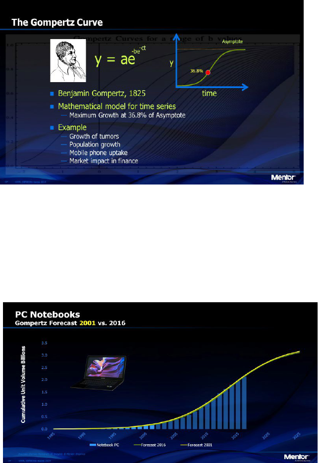
310
Figure 4. The Gompertz Curve predicts evolution in time.
Just to show an example, Figure 5 shows the evolution of notebook
personal computers. Using only the data available in 2001, an S-Curve can
be predicted. In the same figure, the actual data is shown. The prediction
is remarkably accurate.
Figure 5. Prediction of growth of PC notebook unit volume based upon data
available in 2001 versus actual cumulative unit growth.
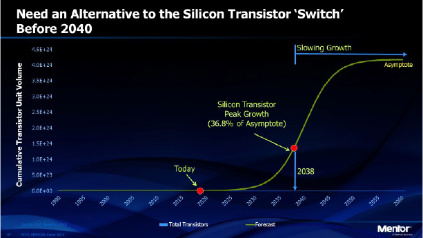
311
One might therefore ask the question, “Where are we in the lifetime
evolution of the silicon transistor?” Figure 6 shows the prediction provided
by the Gompertz formula. The answer is that we have barely begun
producing silicon transistors. If Gompertz is correct, the rate of growth of
production of silicon transistors, in terms of unit volume, will continue to
increase until about 2038 at which time the very high growth rate will peak.
After 2038, the cumulative number of silicon transistors produced will
continue to increase but the rate of increase will slow. By 2050, the annual
increase in the number of silicon transistors produced will asymptotically
approach zero.
Figure 6. Gompertz formula applied to the cumulative number of silicon
transistors manufactured.
While it’s still important to consider alternatives to the silicon transistor,
the immediacy of finding a viable alternative may not be as great as some
might suppose. Meanwhile, we have many opportunities to use those
silicon transistors in new and innovative ways as well as to find new types
of switches as new application needs emerge.
— Dr. Walden Rhines, June 2019
